
Bidirectional semiconductor discharge tube and preparation method thereof

A discharge tube and semiconductor technology, applied in semiconductor/solid-state device manufacturing, semiconductor devices, circuits, etc., can solve problems such as signal distortion

Active Publication Date: 2020-01-24
深圳市德芯半导体技术有限公司
View PDF6 Cites 2 Cited by
  • Summary
  • Abstract
  • Description
  • Claims
  • Application Information

AI Technical Summary

Problems solved by technology

[0004] The purpose of the present invention is to provide a bidirectional semiconductor discharge tube and its preparation method, aiming to solve the problem that the existing TSS device is easy to cause signal distortion due to its high capacitance in the communication line

Method used


Image

  • Bidirectional semiconductor discharge tube and preparation method thereof
  • Bidirectional semiconductor discharge tube and preparation method thereof
  • Bidirectional semiconductor discharge tube and preparation method thereof

Examples


preparation example Construction

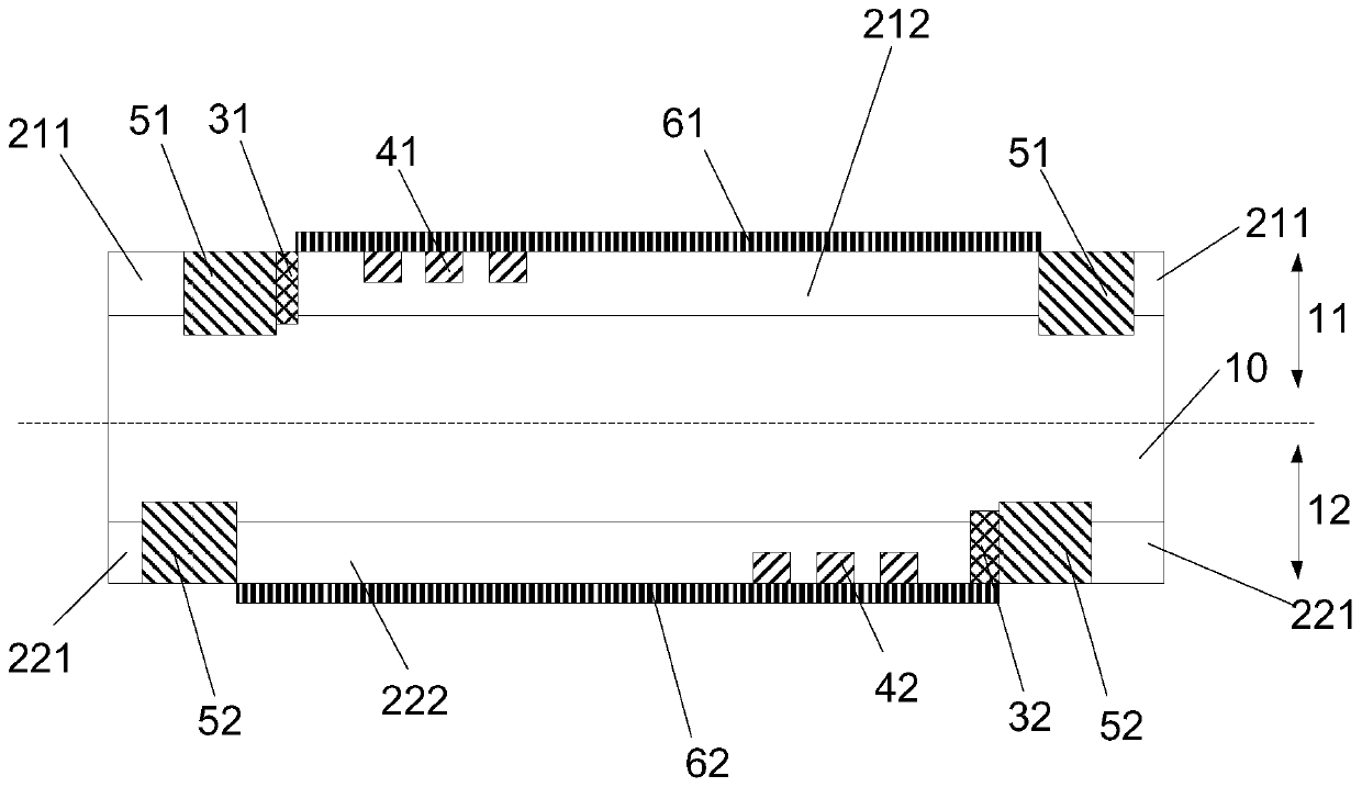
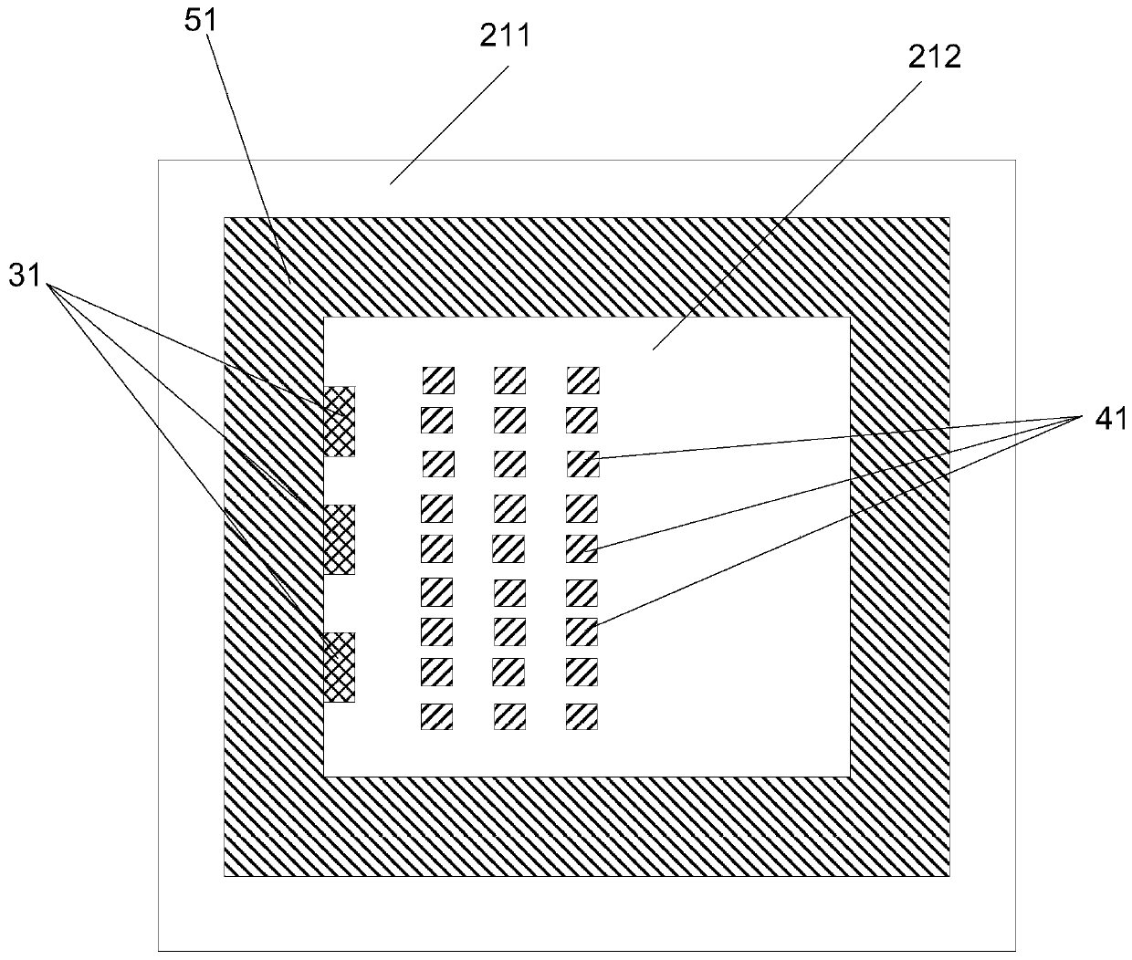
[0053] In one embodiment, this embodiment also provides a method for preparing a bidirectional semiconductor discharge tube. For a schematic cross-sectional structure diagram of a bidirectional semiconductor discharge tube, see figure 1 As shown, the bidirectional semiconductor discharge tube includes a substrate layer 10 having a first conductivity type and a first device layer 11 and a second device layer 12 respectively arranged on both sides of the substrate layer 10, the first device layer 11 The structure of the second device layer 12 is arranged symmetrically, and the preparation method of the first device layer 11 and the second device layer 12 is the same, and the preparation method includes:

[0054] Step a: Form a diffusion layer 21 with a second conductivity type on one side of the substrate layer 10 with the first conductivity type, see image 3 shown.

[0055] In this embodiment, the diffusion layer 21 is formed on the surface of the substrate layer 10 by doping...


PUM


Abstract

The invention belongs to the technical field of semiconductor devices and provides a bidirectional semiconductor discharge tube and a preparation method thereof. The bidirectional semiconductor discharge tube comprises a substrate layer, and a first device layer and a second device layer which are respectively arranged at two sides of the substrate layer; and the structures of the first device layer and the second device layer are symmetrically arranged; the first device layer comprises a diffusion layer, an isolation layer, a metal layer, a plurality of cathode regions, and a heavily doped region; the diffusion layer has a second conductivity type; the isolation layer is used for dividing the diffusion layer into a valid anode region and an invalid anode region; the plurality of cathode regions have a first conductivity type; the heavily doped region is arranged between the valid anode region and the isolation layer; and the heavily doped region has a first conductivity type. According to the bidirectional semiconductor discharge tube and the preparation method thereof of the invention, the heavily doped region with the doping concentration greater than the doping concentration ofthe substrate layer is arranged between the valid anode region and the isolation layer, so that the bidirectional semiconductor discharge tube still has a low capacitance capability when meeting a breakdown voltage, and the problem that signal distortion is easily caused by high capacitance of a TSS device in a communication line is solved.

Description

technical field [0001] The invention relates to the technical field of semiconductor devices, in particular to a bidirectional semiconductor discharge tube and a preparation method thereof. Background technique [0002] TSS (Thyristor Surge Suppressor, voltage switching transient suppression diode) is also called a semiconductor discharge tube, or a solid discharge tube, etc., because TSS can absorb voltage shocks and voltage surges, it plays an important role in the lightning protection of signal circuits Function, its working principle is similar to that of a gas discharge tube. When the overvoltage at both ends of the TSS exceeds the breakdown voltage of the TSS, the TSS clamps the overvoltage to a potential lower than the breakdown voltage close to 0V, and then the TSS continues this Short-circuit state, until the overcurrent flowing through TSS drops below the critical value, TSS returns to open-circuit state. As an important component, TSS can not only absorb the indu...

Claims


Application Information

Patent Timeline
Patent Type & Authority Applications(China)
IPC IPC(8): H01L29/06H01L21/332H01L29/74
CPCH01L29/74H01L29/0688H01L29/0642H01L29/66363Y02P70/50
Inventor 张潘德赖首雄蓝浩涛
Owner 深圳市德芯半导体技术有限公司
Learn More