Optical modulator

An optical modulator and optical transmission technology, used in instruments, optics, nonlinear optics, etc., can solve the problems of large size, low efficiency, and high energy consumption of devices

Inactive Publication Date: 2020-01-31
SHENZHEN UNIV
View PDF8 Cites 1 Cited by
  • Summary
  • Abstract
  • Description
  • Claims
  • Application Information

AI Technical Summary

Problems solved by technology

Many graphene-based modulators mainly use the evanescent field interaction between graphene and waveguide, which has low efficiency and is not conducive to improving the extinction ratio of the modulator.
Although the interaction b

Method used


Image

  • Optical modulator
  • Optical modulator
  • Optical modulator

Examples


Embodiment 1

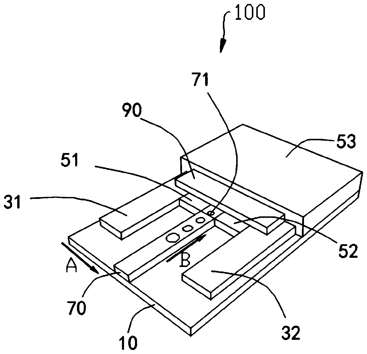
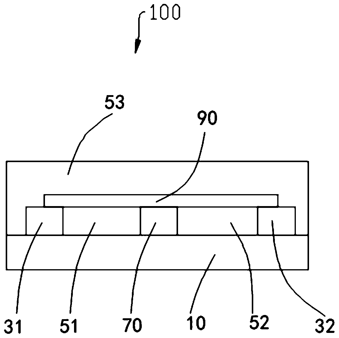
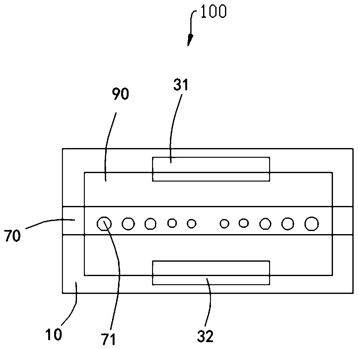
[0075] The optical modulator 100 based on black phosphorous in this embodiment includes a substrate 10, a first electrode 31, a second electrode 32, a first protection member 51, a second protection member 52, a waveguide 70, a thermal layer 90 and a third protection member. piece 53. The first electrode 31, the first protection member 51, the waveguide 70, the second protection member 53, and the second electrode 31 are along the first direction (such as figure 1 Arrow A) are arranged in sequence and arranged on the substrate 10. The waveguide 70 is provided with along the light transmission direction (such as figure 1 Arrow B) arranged through holes 71. The first direction is perpendicular to the light transmission direction. The thermal layer 90 at least partially covers the first electrode 31 and the second electrode 32, and completely covers the through hole 71; the third protection member 53 is formed on the thermal layer 90, and completely covers the first electrode ...

Embodiment 2

[0079] The optical modulator 100 based on black phosphorous in this embodiment includes a substrate 10, a first electrode 31, a second electrode 32, a first protection member 51, a second protection member 52, a waveguide 70, a thermal layer 90 and a third protection member. piece 53. The first electrode 31, the first protection member 51, the waveguide 70, the second protection member 53, and the second electrode 31 are along the first direction (such as figure 1 Arrow A) are arranged in sequence and arranged on the substrate 10. The waveguide 70 is provided with along the light transmission direction (such as figure 1 Arrow B) arranged through holes 71. The first direction is perpendicular to the light transmission direction. The thermal layer 90 at least partially covers the first electrode 31 and the second electrode 32, and completely covers the through hole 71; the third protection member 53 is formed on the thermal layer 90, and completely covers the first electrode ...


PUM

PropertyMeasurementUnit
Widthaaaaaaaaaa
Lengthaaaaaaaaaa

Abstract

The invention relates to an optical modulator. The optical modulator comprises a substrate, a first electrode, a second electrode, a waveguide and a heat-inducing layer, wherein the first electrode, the second electrode and the waveguide are arranged on the same surface of the substrate at intervals; one end of the heat-inducing layer is connected with the first electrode, and the other end of theheat-inducing layer is connected with the second electrode; sequentially arranged through holes are arranged on the waveguide along an optical transmission direction; the heat-inducing layer at leastcovers the through holes, and the heat-inducing layer is used for converting electric energy of an external electric field into heat energy, so that the temperature of each of the heat-inducing layerand the temperature of the waveguide is increased, the refractive indexes of the waveguide and the heat-inducing layer or the waveguide are changed, the intensity of light transmitting through the waveguide is changed, and the regulation and control of a light spectrum are realized. The optical modulator disclosed by the invention has high modulation depth, small device area, and less energy consumption.

Description

technical field [0001] The present invention relates to the field of optoelectronic technology, and more specifically, to an optical modulator. Background technique [0002] Electro-optic modulators are widely used as important key functional devices in communication systems. Traditional electro-optic modulators, such as inorganic modulators and III-V semiconductor modulators, have their own advantages and disadvantages. [0003] Two-dimensional materials represented by graphene and black phosphorus have physical and chemical properties that are difficult for traditional three-dimensional conventional materials. For example, the band gap of black phosphorus changes with the number of layers, and it has ultra-high carrier mobility and strong thermal Light effects, etc., these properties make it possible to use high-performance electro-optic modulators based on two-dimensional materials. Many graphene-based modulators mainly use the evanescent field interaction between graphe...

Claims


Application Information

Patent Timeline
IPC IPC(8): G02F1/01
CPCG02F1/0147
Inventor 张晗陈兴罗小玲
Owner SHENZHEN UNIV
Why Eureka
Try Eureka