
Recovery method of epitaxial growth reaction cavity of light-emitting diode and epitaxial growth method of light-emitting diode

A technology of light-emitting diodes and recovery methods, which is applied to electrical components, circuits, semiconductor devices, etc., can solve problems such as interference in the growth process of epitaxial wafers, and achieve the effect of improving production quality and production efficiency

Active Publication Date: 2020-01-31
HC SEMITEK SUZHOU
View PDF9 Cites 1 Cited by
  • Summary
  • Abstract
  • Description
  • Claims
  • Application Information

AI Technical Summary

Problems solved by technology

However, after the reaction product is cleaned up, the inner wall of the reaction chamber made of metal material will react with the source material, which will interfere with the growth process of the epitaxial wafer

Method used


Image

  • Recovery method of epitaxial growth reaction cavity of light-emitting diode and epitaxial growth method of light-emitting diode
  • Recovery method of epitaxial growth reaction cavity of light-emitting diode and epitaxial growth method of light-emitting diode

Examples


Embodiment Construction

[0034] In order to make the object, technical solution and advantages of the present invention clearer, the implementation manner of the present invention will be further described in detail below in conjunction with the accompanying drawings.

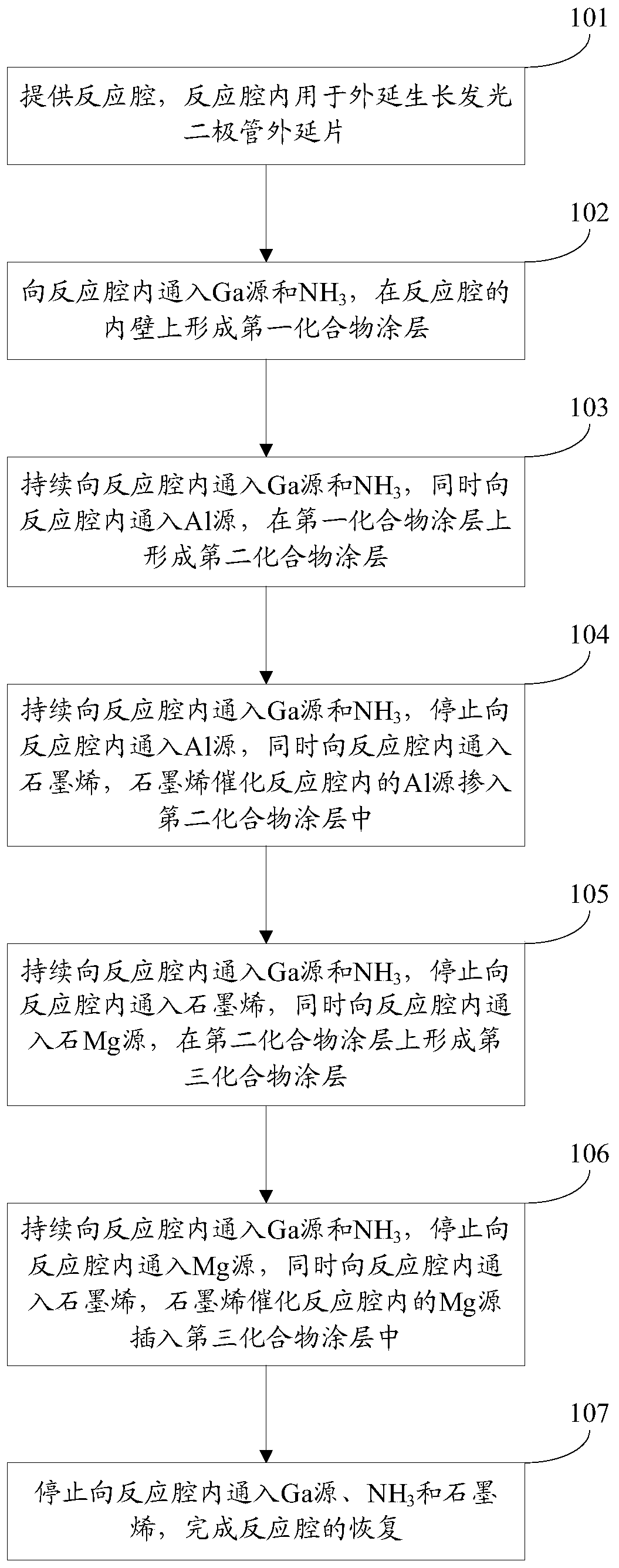
[0035] An embodiment of the present invention provides a recovery method for an epitaxial growth reaction chamber of a light emitting diode. figure 1 It is a flowchart of a recovery method for a light emitting diode epitaxial growth reaction chamber provided by an embodiment of the present invention. see figure 1 , recovery methods include:

[0036] Step 101: providing a reaction chamber for epitaxially growing light-emitting diode epitaxial wafers in the reaction chamber.

[0037] In this embodiment, the reaction chamber may be a reaction chamber of an MOCVD device.

[0038] In practical applications, no epitaxial growth is performed in the reaction chamber, and no reaction product accumulates, or the reaction product has been clea...


PUM


Abstract

The invention discloses a recovery method of the epitaxial growth reaction cavity of a light-emitting diode and an epitaxial growth method of the light-emitting diode and belongs to the technical field of semiconductors. The recovery method comprises the following steps that: a Ga source and NH3 are introduced into a reaction cavity, so that a first compound coating can be formed; an Al source isintroduced into the reaction cavity, so that a second compound coating can be formed; the introduction of the Al source into the reaction cavity is stopped, graphene is introduced into the reaction cavity to the catalyze doping of the Al source into the second compound coating in the reaction cavity; the introduction of the graphene into the reaction cavity is stopped, and a stone Mg source is introduced into the reaction cavity to form a third compound coating; the introduction of the Mg source into the reaction cavity is stopped, graphene is introduced into the reaction cavity to catalyze the doping of the Mg source into the third compound coating in the reaction cavity; and the introduction of the Ga source, NH3 and graphene into the reaction cavity is stopped, so that the recovery of the reaction cavity is finished. With the recovery method of the method adopted, an excellent environment required by the normal growth of the reaction cavity is rapidly recovered, and finally the growth efficiency of MOCVD (metal organic chemical vapor deposition) and product quality are improved.

Description

technical field [0001] The invention relates to the technical field of semiconductors, in particular to a recovery method of a light-emitting diode epitaxial growth reaction chamber and an epitaxial growth method thereof. Background technique [0002] A light-emitting diode (English: Light Emitting Diode, referred to as: LED) is a semiconductor electronic device that can emit light. As a high-efficiency, environmentally friendly and green new solid-state lighting source, LED is being rapidly and widely used in fields such as traffic lights, car interior and exterior lights, urban landscape lighting, and mobile phone backlights. It is a promising new generation of light sources. [0003] The epitaxial wafer is the primary product in the LED manufacturing process, and is usually prepared by Metal Organic Chemical Vapor Deposition (English: Metal organic Chemical Vapor Deposition, abbreviated: MOCVD) equipment. The MOCVD equipment is equipped with a reaction chamber. The subst...

Claims


Application Information

Patent Timeline
Patent Type & Authority Applications(China)
IPC IPC(8): H01L33/00
CPCH01L33/005
Inventor 从颖姚振胡加辉李鹏
Owner HC SEMITEK SUZHOU
Learn More