Chip transfer method and semiconductor device

A chip transfer and chip technology, applied in the direction of semiconductor devices, semiconductor/solid-state device manufacturing, electric solid-state devices, etc., can solve the problems of reducing the life of the adapter, affecting the accuracy of the adapter, and low production efficiency, so as to reduce the technical threshold and cost, improve transfer yield, simple design effect

Active Publication Date: 2020-02-11
BOE TECH GRP CO LTD
View PDF12 Cites 6 Cited by
  • Summary
  • Abstract
  • Description
  • Claims
  • Application Information

AI Technical Summary

Problems solved by technology

[0003] Generally, if the chips transferred in batches are to be soldered to form an electrical connection with the substrate, the substrate or the adapter usually needs to have a heating function. If you choose to use a transfer technology that does not have a heating function, such as stamp transfer, the structure of the chip will be limited. It is difficult to choose a flip-chip (flip-chip) or vertical (vertical) structure. In addition, even if the adapter can be heated, in the case of high precision requirements for micro chip alignment, it may also cause expansion and deformation due to heating. error
[0004] Furthermore, the general adapters are smaller than the size of the substrate, and the entire substrate usually needs to be transferred multiple times, and the transfer process that requires heating and cooling each time will also cause low production efficiency.
[0005] In the prior art, in the patent application with the publication number US201302100194, a MEMS structure adapter is disclosed, which has a heating function, and the substrate can also be heated. After the adapter chip is connected to the substrate, the solder joints are melted by heating the adapter and the substrate. When the chip is connected to the substrate, this method needs to go through the micro-electromechanical process of precision machining on the adapter part, which is difficult and costly to design, and the process of expansion and deformation caused by heating is possible in the micro chip assembly process with a size of only a few microns. Cause alignment errors. In addition, the substrate usually needs to go through multiple transfer processes to assemble a large display panel. If heating and cooling are required for each transfer, it will not only take a long time but also may affect the accuracy of the transfer joint. degree, reducing the life of the adapter
[0006] In the patent application with the publication number TW201705532A, a method of transferring batches of stamps is disclosed. Although the cost of this method is low, the stamps made of polymer molds cannot have built-in heating coils to realize the heating function. If it is heated by external force, there will be a limitation that the stamp is not resistant to high temperature. Therefore, the micro-components transferred to the substrate by this method can only have a horizontal structure, and the adhesive material at the connection with the substrate does not have electrical connection characteristics and can only be fixed. After all the micro-components are transferred to the substrate, it is necessary to make traces on the top of the components by yellow light development again to make them electrically connected to the substrate. However, if the micro-components transferred by this method are light-emitting diodes, the Most of the light-emitting surface will be covered by wires, which will reduce the light-emitting efficiency, and because the wires need to grow along the chip, if the chip is too thick or the electric bond angle is too shaken, the wires will not be able to climb or even break. Thickness and key angles are thus limited

Method used


Image

  • Chip transfer method and semiconductor device
  • Chip transfer method and semiconductor device
  • Chip transfer method and semiconductor device

Examples


Embodiment Construction

[0056]In order to illustrate the present invention more clearly, the present invention will be further described below in conjunction with preferred embodiments and accompanying drawings. Similar parts in the figures are denoted by the same reference numerals. Those skilled in the art should understand that the content specifically described below is illustrative rather than restrictive, and should not limit the protection scope of the present invention.

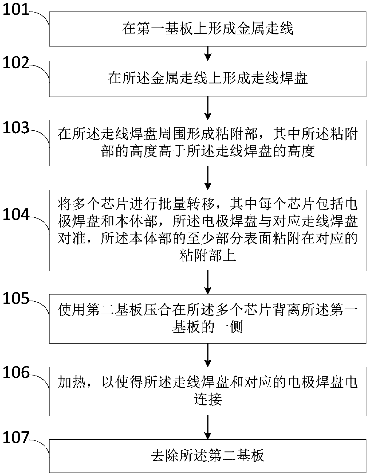
[0057] figure 1 A flow chart showing a chip transfer method proposed by an embodiment of the present invention, such as figure 1 As shown, the method includes the following steps:

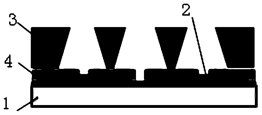
[0058] S101, forming metal wiring on the first substrate;

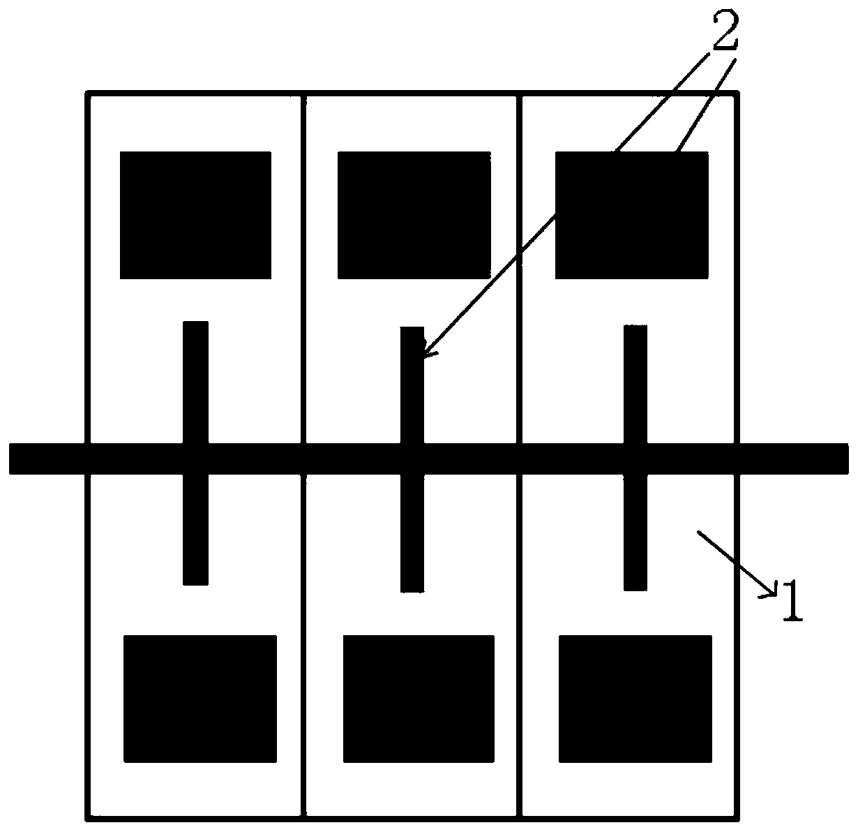
[0059] S102, forming a wiring pad on the metal wiring;

[0060] S103, forming an adhesion part around the wiring pad, wherein the height of the adhesion part is higher than the height of the wiring pad;

[0061] S104. Transfer a plurality of chips in batches, wherein each chip inclu...


PUM


Abstract

The invention discloses a chip transfer method, which includes the following steps: forming a metal wire on a first substrate; forming a wire bonding pad on the metal wire; forming an adhesive portionaround the wire bonding pad, wherein the height of the adhesive portion is greater than the height of the wire bonding pad; transferring a plurality of chips in batches, wherein each chip includes anelectrode bonding pad and a body portion, the electrode bonding pad is aligned to the corresponding wire bonding pad, and at least a part of the surface of the body portion is attached to the corresponding adhesive portion; pressing a second substrate against the sides of the plurality of chips away from the first substrate; performing heating to electrically connect the wire bonding pad to the corresponding electrode bonding pad; and removing the second substrate. The method solves the bonding problem when the chips are transferred to the substrate, can not only reduce the technical threshold and cost of a transfer device, but also can improve the transfer yield without an increase in cost.

Description

technical field [0001] The invention relates to the field of display technology. More specifically, it relates to a chip transfer method and a semiconductor device. Background technique [0002] Micro display technology is a new display technology in recent years. Although it has the advantages of self-illumination, low power consumption, and high color saturation, there are still many problems to be overcome in terms of batch transfer and chip structure efficiency since its development. Various manufacturers and researchers Each unit also proposes a different solution. [0003] Generally, if the chips transferred in batches are to be soldered to form an electrical connection with the substrate, the substrate or the adapter usually needs to have a heating function. If you choose to use a transfer technology that does not have a heating function, such as stamp transfer, the structure of the chip will be limited. It is difficult to choose a flip-chip (flip-chip) or vertical ...

Claims


Application Information

Patent Timeline
Patent Type & Authority Applications(China)
IPC IPC(8): H01L21/683H01L33/62H01L25/075
CPCH01L21/6835H01L33/62H01L25/0753H01L2221/68372H01L2933/0066
Inventor 刘超董恩凯翟明李沛孙海威
Owner BOE TECH GRP CO LTD
Why Eureka
Try Eureka