Miniature ultra-low capacitance solid discharge tube and manufacturing method thereof

A solid discharge tube, ultra-low technology, applied in circuits, thyristors, electrical components, etc., can solve the problem of insufficient chip area

Pending Publication Date: 2020-02-11
江苏东晨电子科技有限公司
View PDF0 Cites 4 Cited by
  • Summary
  • Abstract
  • Description
  • Claims
  • Application Information

AI Technical Summary

Problems solved by technology

[0004] The purpose of the present invention is to solve the problem that the current low-capacitance structure cannot realize the parasitic capacitance below 15pF, and the current chip area cannot meet the tiny SOT-23 inte

Method used


Image

  • Miniature ultra-low capacitance solid discharge tube and manufacturing method thereof
  • Miniature ultra-low capacitance solid discharge tube and manufacturing method thereof
  • Miniature ultra-low capacitance solid discharge tube and manufacturing method thereof

Examples


Embodiment Construction

[0027] The present invention will be further described below in conjunction with the accompanying drawings and embodiments.

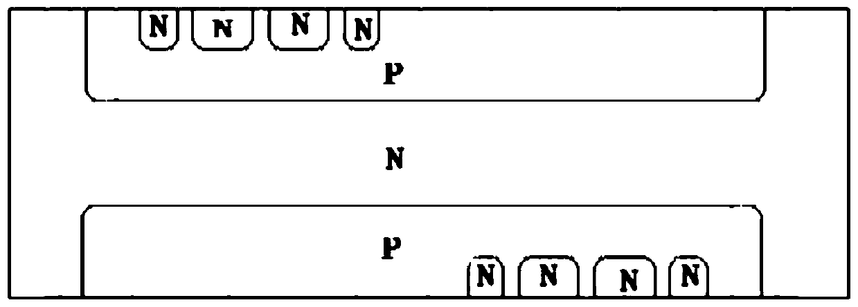
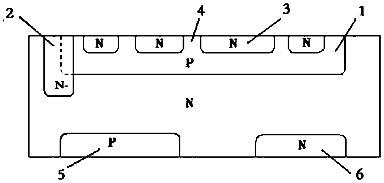
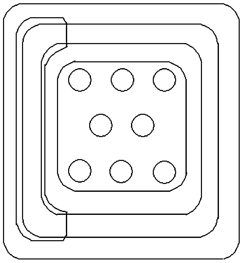
[0028] A miniature ultra-low capacitance solid discharge tube, the microchip area is 0.56mm*0.56mm, such as figure 2 , 3 As shown, it includes the upper boron-based region P1 and the lower boron-based region P5, and a phosphorus diffusion region N+3 is respectively arranged in the upper boron-based region P1 to form a cellular cathode; the boron-based region P1 and the boron-based region P5 The junction depth is 20--25μm. A boron region P5 and a second phosphorus diffusion region N+6 are arranged below, and the positions of the two regions are independently laid out, and the junction depth of the boron region is 20--25μm.

[0029] In the present invention, the junction capacitance of the ultra-low capacitance is less than 6pF.

[0030] In the present invention, a metal layer is provided on the outside of the upper boron base region P1 and the lower ...


PUM

PropertyMeasurementUnit
Junction capacitanceaaaaaaaaaa
Areaaaaaaaaaaa

Abstract

The invention discloses a miniature ultra-low capacitance solid discharge tube and a manufacturing method thereof. A boron-based region P is arranged on the solid discharge tube, a phosphorus diffusion buried layer N- which is partially overlapped is arranged on one side of the boron-based region P, a first phosphorus diffusion region N+ is arranged in the boron-based region P, and a plurality ofshort-circuit holes are arranged in the first phosphorus diffusion region N + to form a cellular cathode. A boron region P and a second phosphorus diffusion region N+ are arranged below the solid discharge tube, and the boron region P and the second phosphorus diffusion region N+ are arranged at intervals to form a one-way chip anode structure. In the invention, on the basis of an original low-capacitance structure design, a N- buried layer is added to the cathode so that heat sink of each cellular cathode is increased, and a flow capacity is improved on the basis of a same chip area. A boronregion and a second phosphorus diffusion region N+ are arranged in an symmetrical mode, reverse voltage drop of a single discharge tube is eliminated, and based on the design, an area of an original chip can be reduced so that the area of a PN junction is reduced, and a junction capacitance is greatly decreased.

Description

technical field [0001] The invention relates to the design and manufacture of semiconductor chips, in particular to a miniature ultra-low capacitance solid discharge tube. Background technique [0002] At present, the withstand voltage control of conventional low-voltage solid discharge tubes (below 64V) can achieve consistency within 5V, which can fully meet the current client line requirements. However, as the data transmission rate of customer application lines is getting higher and higher , the design power consumption of circuit boards is getting lower and lower, so low-voltage, small-volume, and highly integrated solid protection devices are more and more widely used, but the junction capacitance of low-voltage solid protection devices with the same lightning strike level is generally higher by 25~ 30pF, because the high junction capacitance will affect the quality of data transmission, and the junction capacitance will cause packet loss in the transmission of digital ...

Claims


Application Information

Patent Timeline
IPC IPC(8): H01L29/74H01L29/08
CPCH01L29/0839H01L29/74
Inventor 陈俊标苏亮沈一舟
Owner 江苏东晨电子科技有限公司
Why Eureka
Try Eureka