Display panel suitable for under-screen camera

A display panel and camera technology, which is applied in the manufacture of electrical components, electrical solid-state devices, semiconductor/solid-state devices, etc., can solve problems such as poor color purity, conflict between color purity and transmittance requirements, and influence of AMOLED screen transmittance. , to achieve superior performance

Inactive Publication Date: 2020-02-11
FUDAN UNIV
View PDF4 Cites 16 Cited by
  • Summary
  • Abstract
  • Description
  • Claims
  • Application Information

AI Technical Summary

Problems solved by technology

In this way, there is a dilemma in the requirements for the cathode in actual production: if the cathode is too thin and the microcavity effect is too weak, it will show a relatively wide spectrum inherent to OLED, and the spectrum has shoulder peaks, and the spectrum cannot be narrowed. If the cathode is too thick, the transmittance of the AMOLED screen will be affected ( image 3 )
Since different areas of the OLED display screen have different requirements for screen transmittance, the color purity brought about by the thickness of the OLED cathode conflicts with the transmittance requirements, and the camera effect is poor, requiring a lot of image processing corrections ( Figure 5 )

Method used


Image

  • Display panel suitable for under-screen camera
  • Display panel suitable for under-screen camera
  • Display panel suitable for under-screen camera

Examples


Embodiment 1

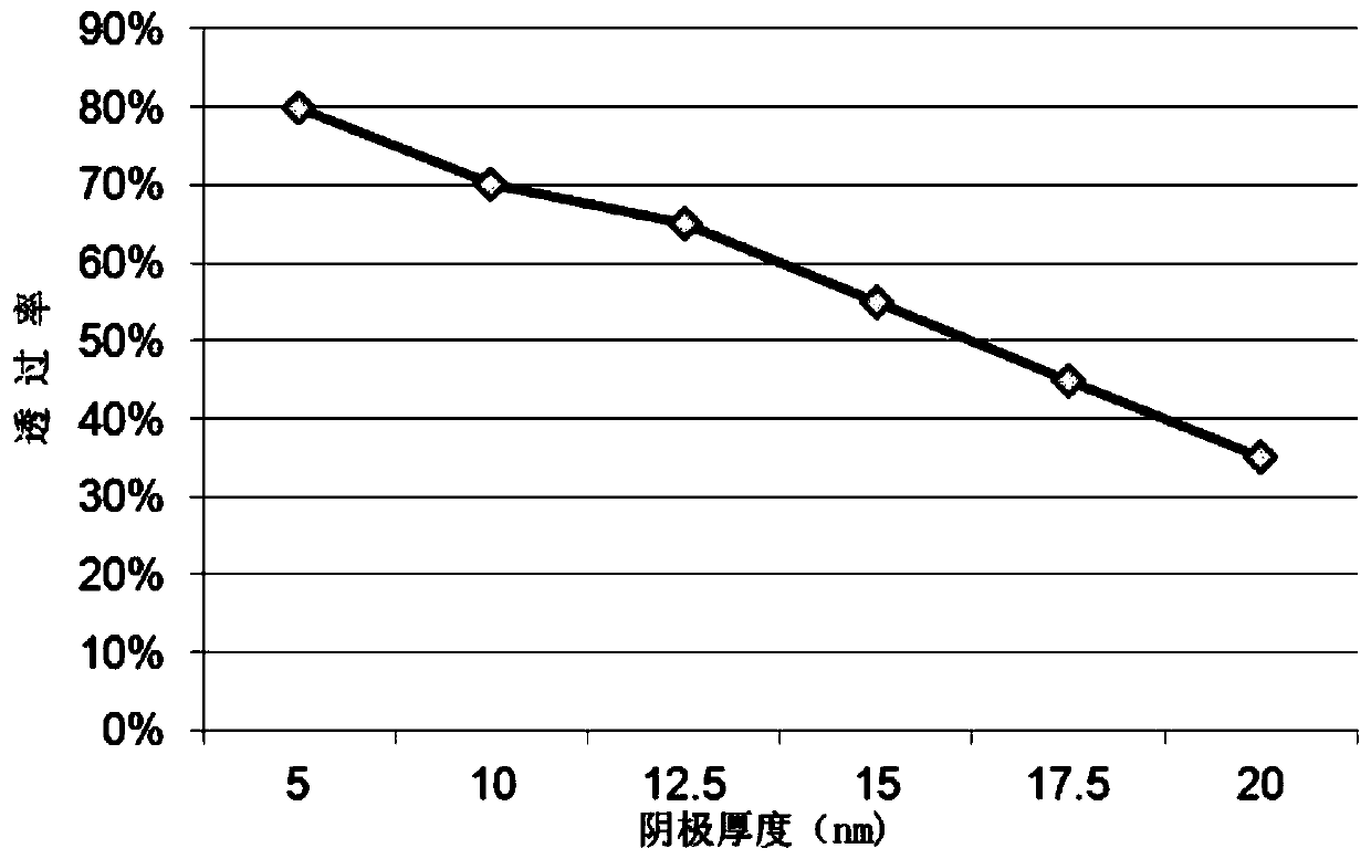
[0047] Such as Figure 9As shown, only the anode E and the display driving backplane F are the same in the display area a and the display area b (the same process), and the hole transport layer, light-emitting layer, electron transport layer, and cathode above the anode are separated, respectively, according to the same light and color performance The requirements match the corresponding functional film layer, in which the cathode A1 is an ultra-thin structure (the transmittance is greater than 70%), and the cathode A2 is a semi-permeable structure (the transmittance is between 35% and 55%).

[0048] The characteristics of this solution: the display backplane and driving scheme of area a and b are consistent with the traditional ones, and the display panels with the same light and color performance are matched by using their respective diode structure differences.

Embodiment 2

[0050] Such as Figure 10 As shown, the electron transport layer B, the hole transport layer D, the anode E and the display drive backplane F in the display a area are the same as the display b area (the same process), and the light-emitting layer and the cathode are separated from each other. Due to the quantum dot device in the a area The OLED device in area b shows a slight difference in voltage driving, and uses the difference compensation balance of driving signals in area a and area b. This signal includes power signal VDD, VEE, and data signal Vdata, etc.; the cathode A1 is an ultra-thin structure ( The transmittance is greater than 70%), and the cathode A2 is a semi-permeable structure (the transmittance is between 35% and 55%).

[0051] Features of this scheme: the power-driven backplane, anode, and functional film layer of area a and area b are the same, only the light-emitting layer and cathode are different, and the process is relatively simple; the driving scheme ...

Embodiment 3

[0053] Such as Figure 11 As shown, the electron transport layer B, the hole transport layer D, the anode E and the display drive backplane F in the display a area are the same as the display b area (the same process), and the light-emitting layer and the cathode are separated from each other. Due to the quantum dot device in the a area The OLED device in area b shows a slight difference in voltage driving. Using the pre-experimental selection of light-emitting layer materials in area a and b, the materials for quantum dot light-emitting layer C1 and OLED organic light-emitting layer C2 with similar light and color properties are obtained. For organic functional layer B , D can also be selected through device pre-experimentation; the cathode A1 is an ultra-thin structure (the transmittance is greater than 70%), and the cathode A2 is a semi-permeable structure (the transmittance is between 35% and 55%).

[0054] Features of this solution: the power-driven backplane, anode, and ...


PUM

PropertyMeasurementUnit
diameteraaaaaaaaaa

Abstract

The invention discloses a display panel suitable for an under-screen camera. The display panel comprises a driving back plate, an anode, a hole transport layer, a light emitting layer, an electron transport layer and a cathode. The display panel is divided into a display area a and a display area b; the cathode of the display area a is a high-transmittance cathode, the light emitting layer is a quantum dot light emitting layer, and an under-screen camera is arranged below the display area a; the cathode of the display area b is a low-transmittance cathode, and the light-emitting layer is an OLED organic light-emitting layer. According to the novel appropriate display device structure of an under-screen camera and a display panel design, high-color-purity display performance and high transparency of the camera area can be achieved at the same time and a true full screen with excellent performance is realized.

Description

technical field [0001] The invention belongs to the field of display technology, and in particular relates to a display panel suitable for an under-display camera. Background technique [0002] Due to the broad intrinsic spectrum of OLED, the spectrum has shoulder peaks, the spectrum cannot be narrowed, and the color purity is not good. Therefore, AMOLED mobile phones and wearable products now adopt the top-emitting AMOLED device structure, that is, the light of the organic light-emitting layer is emitted from the cathode side, and the cathode has a certain degree of impermeability, thereby forming an optical microcavity between the electrodes, and the light in the microcavity The medium vibration is coupled to narrow the spectrum to meet the daily needs of high color purity consumer products ( figure 1 , figure 2 ). [0003] In specific design and production, increasing the thickness of the cathode can obtain a narrowed and enhanced spectrum. In this way, there is a di...

Claims


Application Information

Patent Timeline
Patent Type & Authority Applications(China)
IPC IPC(8): H01L51/52H01L27/32
CPCH10K59/12H10K50/82
Inventor 熊志勇梅时良解凤贤张万路郭睿倩张国旗
Owner FUDAN UNIV
Why Eureka
Try Eureka