Supercharge Your Innovation With Domain-Expert AI Agents!

Layered AMOLED pixel compensation circuit

A compensation circuit, layered technology, applied in the direction of circuits, electrical components, electrical solid-state devices, etc., can solve the problems of reduced quantity, increased area occupied by Pixels, and uneven brightness of the panel, so as to reduce the occupied area, The effect of increasing the resolution

Pending Publication Date: 2020-02-21
FUJIAN HUAJIACAI CO LTD
View PDF0 Cites 0 Cited by
  • Summary
  • Abstract
  • Description
  • Claims
  • Application Information

AI Technical Summary

Problems solved by technology

For OLED panels, the in-plane 2T1C Pixel circuit will be affected by Vth drift, resulting in uneven brightness of the panel. A compensation circuit is needed to improve the display effect of the panel. In order to achieve a better compensation effect, the compensation circuit will have multiple TFTs, which may There will be 4T, 5T, 6T..., so too many TFTs will increase the area occupied by the Pixel, which will lead to a decrease in the number of Pixels that the panel can accommodate, that is, the resolution becomes lower, which cannot meet the high-resolution requirements

Method used


Image

  • Layered AMOLED pixel compensation circuit
  • Layered AMOLED pixel compensation circuit
  • Layered AMOLED pixel compensation circuit

Examples


Embodiment Construction

[0029] In order to explain in detail the technical content, structural features, achieved goals and effects of the technical solution, the following will be described in detail in conjunction with specific embodiments and accompanying drawings.

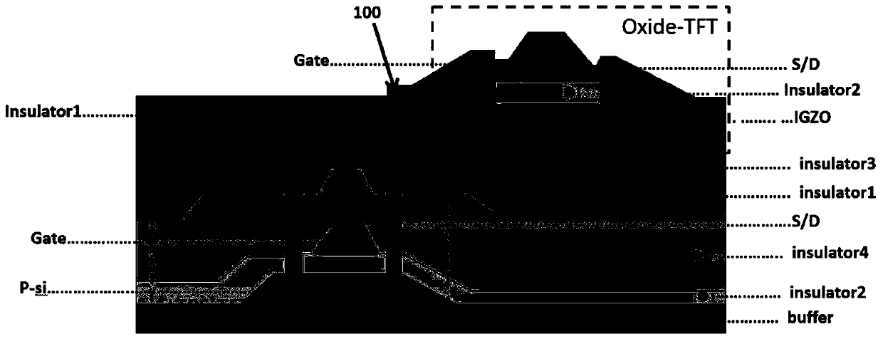
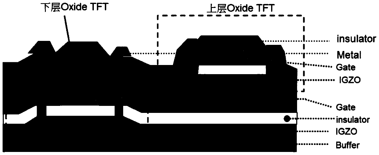
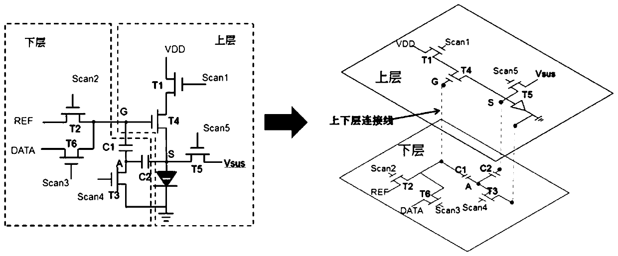
[0030] see figure 1 , a layered AMOLED pixel compensation circuit, such as figure 1 As shown, in the pixel compensation circuit, including the lower thin film transistor region and the upper thin film transistor region arranged on the substrate buffer, an insulating layer (Insulator1) is also arranged between the upper thin film transistor region and the lower thin film transistor region, and the insulating layer can be Silicon oxide film is used. The electrode of the upper thin film transistor region is connected to the electrode of the lower thin film transistor region through the connecting line 100 passing through the insulating layer, and the upper thin film transistor region is also patterned with an organic light emitting diod...


PUM


Abstract

The invention relates to a layered AMOLED pixel compensation circuit. The array substrate comprises a lower-layer thin film transistor area and an upper-layer thin film transistor area which are arranged on a substrate, and an insulating layer is further arranged between the upper-layer thin film transistor area and the lower-layer thin film transistor area. The electrode of the upper-layer thin film transistor region is connected with the electrode of the lower-layer thin film transistor region through a connecting wire penetrating through the insulating layer; an organic light-emitting diodeis further patterned in the upper-layer thin film transistor area, and the thin film transistor in the upper-layer thin film transistor area and the thin film transistor in the lower-layer thin filmtransistor area are connected to form a compensation circuit of the organic light-emitting diode. Different from the prior art, the technical scheme has the advantages that different lower-layer thinfilm transistor regions and upper-layer thin film transistor regions on the substrate are designed, and finally, the area occupied by the plurality of thin film transistors of the pixel compensation circuit is reduced in the vertical direction, so that the occupied area of a single pixel is reduced, and finally, the resolution of a screen is improved.

Description

technical field [0001] The invention relates to the design of a pixel compensation circuit, in particular to a novel AMOLED pixel compensation circuit design with upper and lower layers. Background technique [0002] Today, with the continuous improvement of technology, people's requirements for display screens are also increasing, that is, the demand for high resolution is increasing. For example, the resolution of VR, AR, MR and other displays is as high as 2000PPI. For OLED panels, the in-plane 2T1C Pixel circuit will be affected by Vth drift, resulting in uneven brightness of the panel. A compensation circuit is needed to improve the display effect of the panel. In order to achieve a better compensation effect, the compensation circuit will have multiple TFTs, which may There will be 4T, 5T, 6T..., so too many TFTs will increase the area occupied by the Pixel, which will lead to a decrease in the number of Pixels that the panel can accommodate, that is, the resolution wi...

Claims


Application Information

Patent Timeline
IPC IPC(8): G09G3/3225G09G3/3233H01L27/32
CPCG09G3/3225G09G3/3233G09G2320/0233H10K59/123H10K59/1213
Inventor 罗敬凯卢昭阳贾浩
Owner FUJIAN HUAJIACAI CO LTD
Features
  • R&D
  • Intellectual Property
  • Life Sciences
  • Materials
  • Tech Scout
  • Unparalleled Data Quality
  • Higher Quality Content
  • 60% Fewer Hallucinations
Learn More