
Pre-alignment device and silicon wafer pre-alignment method

A pre-alignment, silicon wafer technology, which is applied in photoplate-making process exposure devices, microlithography exposure equipment, electrical components, etc., can solve the problems of increasing the area occupied by the silicon wafer handover robot, unfavorable placement, and larger equipment size. , to improve product adaptability and compatibility, solve fragile, improve safety and productivity

Active Publication Date: 2022-02-15
SHANGHAI MICRO ELECTRONICS EQUIP (GRP) CO LTD
View PDF8 Cites 0 Cited by
  • Summary
  • Abstract
  • Description
  • Claims
  • Application Information

AI Technical Summary

Problems solved by technology

As the thickness of the silicon wafer becomes thinner, the existing pre-alignment device reduces the edge collapse of the silicon wafer by increasing the bearing surface of the rotating carrier plate, but this will increase the occupied area of ​​the silicon wafer handover robot at the same time, making the size of the equipment smaller. large, not conducive to placement

Method used


Image

  • Pre-alignment device and silicon wafer pre-alignment method
  • Pre-alignment device and silicon wafer pre-alignment method
  • Pre-alignment device and silicon wafer pre-alignment method

Examples


Embodiment 1

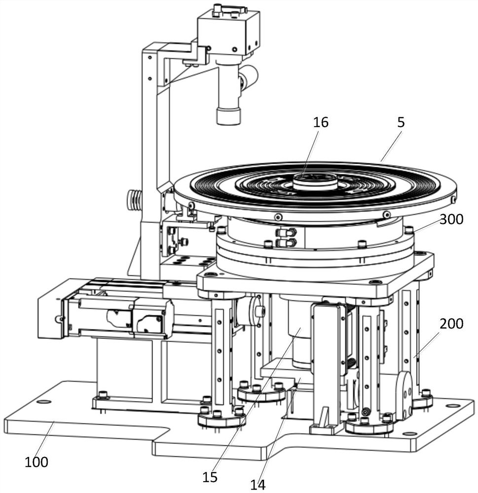
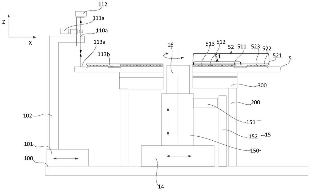
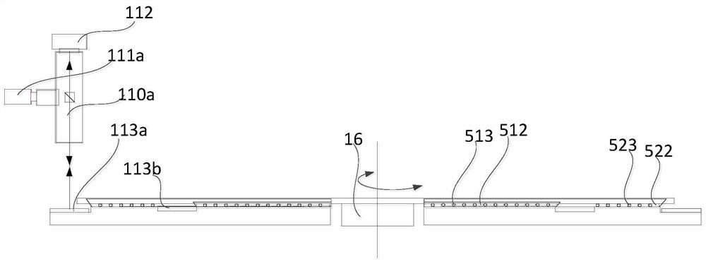
[0080] Please refer to figure 1 and figure 2 , an embodiment of the present invention provides a pre-alignment device, including: a base plate 100, a pre-alignment optical-mechanical unit, a rotary motion unit, a rotary bearing unit, a horizontal position compensation unit 14, a vertical motion unit 15, and a transfer bearing unit 16 .

[0081] The bottom plate 100 is used for installing and supporting the pre-alignment optical-mechanical unit, the rotary motion unit, the rotary bearing unit, the horizontal position compensation unit 14 , the vertical motion unit 15 and the transfer bearing unit 16 .

[0082] The rotating carrying unit includes a hollow carrying tray 5 for carrying silicon wafers and an adsorption assembly for absorbing the silicon wafers. The hollow carrying tray 5 includes a hollow area (not shown) in the center and a The carrying area of ​​the periphery, the hollow area is used to provide the space for the handover carrying unit 16 to be set and moved, t...

Embodiment 2

[0119] Please refer to Figure 5 , in order to be compatible with the reflective pre-alignment method and the through-beam pre-alignment method, another embodiment of the present invention also provides a pre-alignment device, which is compatible with Figure 1 to Figure 4 Compared with the pre-alignment device in the shown embodiment, a set of opposite-type pre-alignment optical-mechanical components is added to the pre-alignment optical-mechanical unit, and the hollow carrying disc is at the outer edge of each carrying area Coating treatment, for example, can realize the function of reflecting the light of the first light source 111 a and transmitting the light of the second light source 111 b in these regions. Specifically, the pre-alignment optomechanical unit 11 in this embodiment includes a first lens 110 a , a second lens 110 b , a first light source 111 a , a second light source 111 b , a mirror 113 c and a camera 112 . Wherein, the installation positions of the first...

Embodiment 3

[0123] In some cases, because the silicon wafer is too thin, the stiffness of the silicon wafer is weakened, even if the silicon wafer is placed in Figure 1 to Figure 5 On the shown pre-alignment device, there is still a certain slump phenomenon in the edge part of the silicon wafer not supported on the hollow carrier tray 5, so in another embodiment of the present invention, please refer to Image 6 , in order to alleviate the problem that the edge of the silicon wafer rests, at least one ring of raised structures for supporting the silicon wafer is arranged on the outside of each suction cup. That is, the pre-alignment device of this embodiment, and Figure 1 to Figure 5 Compared with the pre-alignment device shown, a raised structure located on the outside of each suction cup is added to the hollow carrier plate 5, for example, a ring located on the outside of the first suction cup 511 is provided on the first bearing area 51. The protruding structure 514 is provided with...


PUM


Abstract

The present invention provides a pre-alignment device, which arranges the transfer bearing unit in the hollow area of ​​the hollow bearing plate, and arranges the vertical movement unit and the horizontal position compensation unit which drive the transfer bearing unit to move inside the rotation movement unit, which can make The handover carrying unit shuttles up and down and moves horizontally in the hollow area, thus, while increasing the area of ​​the carrying area of ​​the hollow carrying plate, the size of the equipment can be avoided; the suction cup, the adsorption hole and the The protruding structure used to support the silicon chip can absorb and flatten the silicon chip it carries, thereby solving the problem of fragility during pre-alignment of the ultra-thin silicon chip and improving the pre-alignment accuracy of the ultra-thin silicon chip. The invention also provides a silicon chip pre-alignment method, which uses the pre-alignment device of the invention to realize the silicon chip pre-alignment. The present invention also provides an exposure equipment, a photolithography system, a silicon wafer processing system and a method, which are realized by using the pre-alignment device and the pre-alignment method of the present invention.

Description

technical field [0001] The invention relates to the technical field of semiconductor manufacturing, in particular to a pre-alignment device and a silicon chip pre-alignment method. Background technique [0002] In the semiconductor industry, there are more and more types of silicon wafers that need to be processed, such as standard wafers, warped wafers, ultra-thin wafers, etc. Among them, there are many studies on the treatment methods of standard wafers and warped wafers, but the ultra-thin wafers are easily broken due to the influence of the strength of the silicon wafer itself during adsorption and transportation. In addition, due to the thinning of the silicon wafer thickness, the If the stiffness is weakened, the edge of the silicon wafer will collapse, which will cause defocusing of the silicon wafer during pre-alignment and edge exposure on a machine such as a lithography machine, which will eventually affect the accuracy of silicon wafer pre-alignment and edge expos...

Claims


Application Information

Patent Timeline
Patent Type & Authority Patents(China)
IPC IPC(8): H01L21/68H01L21/67G03F7/20
CPCH01L21/68H01L21/67011G03F7/20
Inventor 王刚付红艳宋海军黄栋梁
Owner SHANGHAI MICRO ELECTRONICS EQUIP (GRP) CO LTD
Learn More