Semiconductor device and forming method thereof

A semiconductor and device technology, applied in the field of semiconductor devices and their formation, can solve problems affecting the performance of semiconductor devices, difficulties, and insufficient filling of metal gates

Pending Publication Date: 2020-03-03
SEMICON MFG INT (SHANGHAI) CORP +1
View PDF5 Cites 0 Cited by
  • Summary
  • Abstract
  • Description
  • Claims
  • Application Information

AI Technical Summary

Problems solved by technology

[0003] Due to the reduction in size, the process of filling materials into narrower grooves becomes more difficult, and there is a situation of insufficient filling. Fo

Method used


Image

  • Semiconductor device and forming method thereof
  • Semiconductor device and forming method thereof
  • Semiconductor device and forming method thereof

Examples


no. 1 example

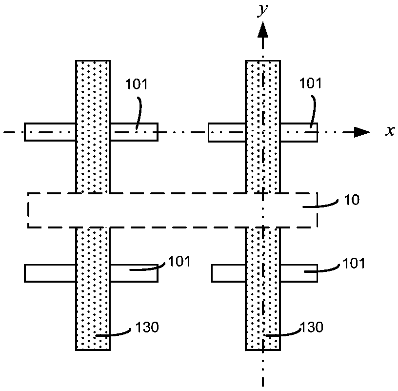
[0043] Please refer to figure 1 , forming a dummy gate 130 on part of the fin portion 101 .

[0044] figure 1 It is a top view of the structure of the embodiment of the present invention, the dummy gate 130 covers part of the fin 101 , and the area framed by the dotted line 10 is the area where the interlayer isolation structure will be formed later.

[0045] figure 1 x and y in represent two different directions of the structure of the embodiment of the present invention respectively. Each of the drawings below includes two parts a and b, and part a and part b are respectively along the figure 1 The structural schematic diagram obtained by the longitudinal section of the y-direction line and the x-direction line in the middle is applicable to different embodiments of the present invention.

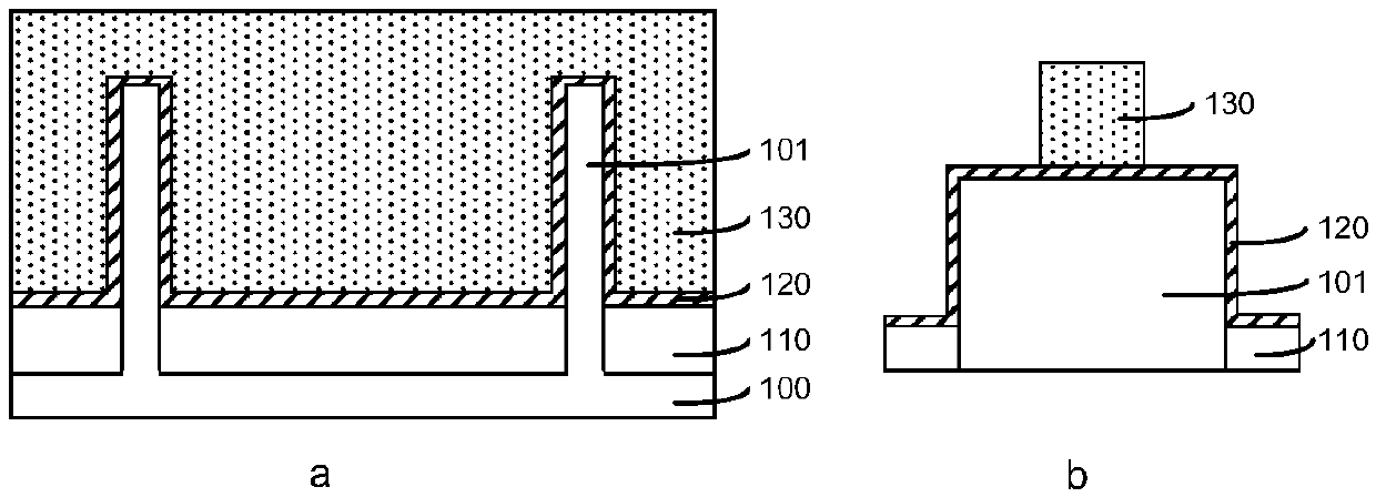
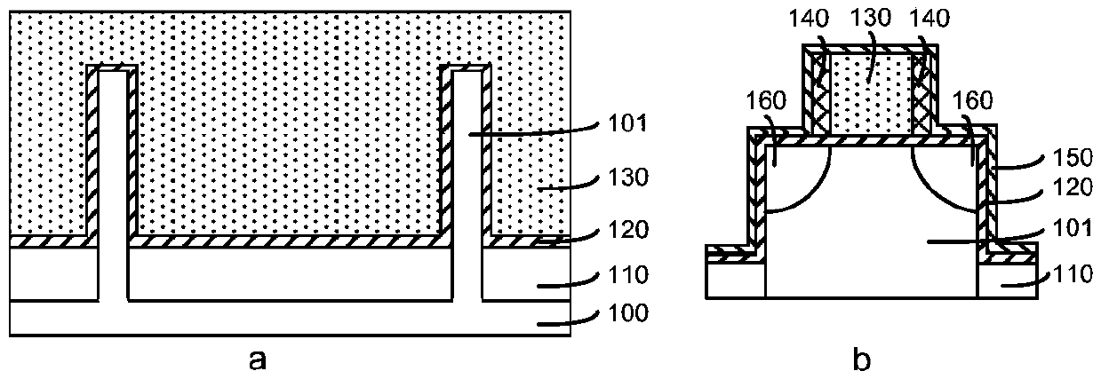
[0046] Please refer to figure 2 A fin portion 101 is formed above the semiconductor substrate 100 , and a dummy gate structure (not shown) is formed on part of the fin portion 101 ....

no. 2 example

[0106] The difference between the second embodiment and the first embodiment is: after removing the dummy gate structure, continue to etch part of the interlayer isolation structure, so that from the bottom of the first sidewall to the bottom of the second sidewall, the The distance between the point and the central axis of the longitudinal section of the fin adjacent to the second side wall decreases. Other process steps are consistent with the first embodiment.

[0107] From providing the semiconductor substrate 200 to removing the dummy gate structure, the process steps of the embodiment of the present invention are consistent with those of the first embodiment, and will not be repeated here.

[0108] Please refer to Figure 10 After the dummy gate structure is removed, a part of the interlayer isolation structure 271 is etched.

[0109] In order to further increase the distance between the interlayer isolation structure 271 and the fin 201 by etching part of the side sur...


PUM

PropertyMeasurementUnit
Thickness dimensionaaaaaaaaaa
Thicknessaaaaaaaaaa

Abstract

The invention further provides a forming method for a semiconductor device. The method comprises the following steps: an interlayer isolation structure is formed in a semiconductor device, wherein theinterlayer isolation structure comprises a first part and a second part, the first part is positioned outside a pseudo gate structure, the second part is covered by the pseudo gate structure, the side wall of the first part and the side wall of the second part are respectively a first side wall and a second side wall, the distance between the top of the first side wall and the central axis of thelongitudinal section of the fin part adjacent to the first side wall is l1, the distance between the bottom of the first side wall and the central axis of the longitudinal section of the fin portionadjacent to the first side wall is l2, the distance between a point on the second side wall on the same side as the first side wall and the central axis of the longitudinal section of the fin part adjacent to the second side wall is l3, and l1 > l2 >/ = l3. The distance between the interlayer isolation structure and the fin part is increased, the metal gate material can be filled easily, and holesare avoided.

Description

technical field [0001] The invention relates to the field of semiconductor manufacturing, in particular to a semiconductor device and a forming method thereof. Background technique [0002] For a long time, reducing the size of transistors and improving the integration of integrated circuits has been the eternal pursuit of the semiconductor industry. From FinFET (Fin Transistor) to NWFET (Nanowire Transistor), the physical size of the gate keeps decreasing. [0003] Due to the reduction in size, the process of filling materials into narrower grooves becomes more difficult, and there is a situation of insufficient filling. For example, when filling the grooves to form metal gates, it is easy to have holes that are not filled with metal gates, which affects semiconductors. device performance. [0004] Therefore, there is an urgent need for a semiconductor device and a method for forming the semiconductor device with fewer holes and improved performance of the semiconductor d...

Claims


Application Information

Patent Timeline
IPC IPC(8): H01L29/06H01L21/336H01L29/78
CPCH01L29/785H01L29/66795H01L29/0642
Inventor 王楠
Owner SEMICON MFG INT (SHANGHAI) CORP
Why Eureka
Try Eureka