

Electronic component
A technology of electronic components and external electrodes, which is applied in the direction of electrical components, circuits, parts of fixed capacitors, etc.
- Summary
- Abstract
- Description
- Claims
- Application Information
AI Technical Summary
Problems solved by technology
Method used
Image

Examples
Embodiment Construction
[0036] Exemplary embodiments of the present disclosure will now be described in detail below with reference to the accompanying drawings.
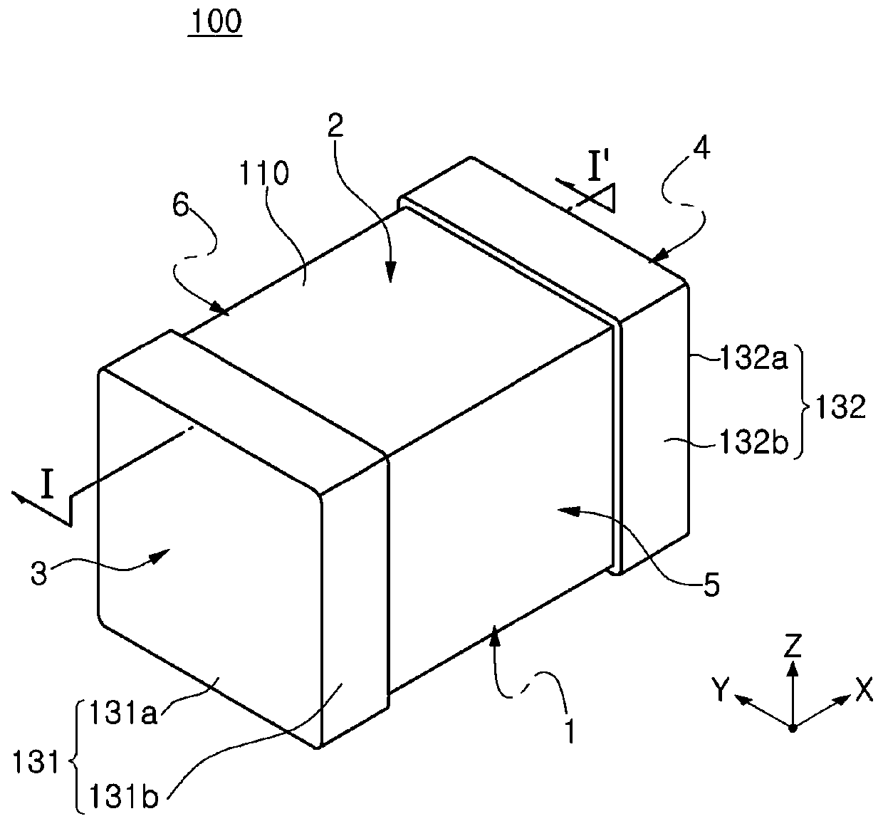
[0037] Directions will be defined to clearly describe exemplary embodiments in the present disclosure. X, Y and Z in the drawings refer to the length direction, width direction and thickness direction of the multilayer capacitor and electronic component, respectively.
[0038] Here, the Z direction refers to the stacking direction along which the dielectric layers are stacked in this exemplary embodiment.
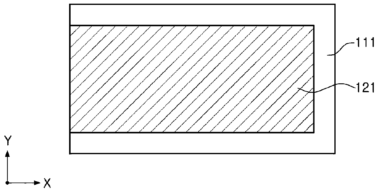
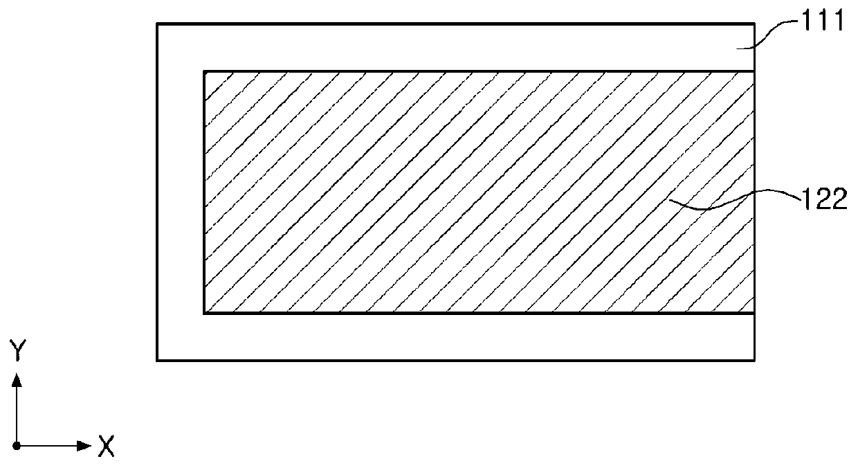
[0039] figure 1 is a perspective view schematically showing a multilayer capacitor applied to an exemplary embodiment in the present disclosure, Figure 2A with Figure 2B is shown applied to figure 1 A plan view of the first internal electrode and the second internal electrode of the multilayer capacitor, image 3 is along figure 1 The cross-sectional view taken along the line II'.
[0040] First, refer to Figure 1 to Figure 3...
PUM
 Abstract
Description
Claims
Application Information