Wafer level packaging method and packaging structure

A technology of wafer-level packaging and packaging methods, which is applied in the manufacturing of electrical components, electrical solid-state devices, semiconductor/solid-state devices, etc., to achieve the effect of simplifying the packaging structure

Active Publication Date: 2020-03-10
NINGBO SEMICON INT CORP
View PDF4 Cites 13 Cited by
  • Summary
  • Abstract
  • Description
  • Claims
  • Application Information

AI Technical Summary

Problems solved by technology

[0005] However, the current WLP method needs to be further simplified

Method used


Image

  • Wafer level packaging method and packaging structure
  • Wafer level packaging method and packaging structure
  • Wafer level packaging method and packaging structure

Examples


Embodiment Construction

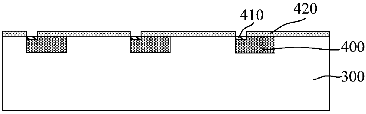
[0031] It can be seen from the background technology that the process of the packaging structure in the prior art is relatively complicated. The reason for the analysis is that in the prior art, after the bare chip to be integrated is bonded to the wafer, a first connection to be electrically connected to the bare chip needs to be formed. structure, the second connection structure electrically connected to the chips in the wafer, and the interconnection structure electrically connected to the first connection structure and the second connection structure, the process is relatively complicated.

[0032] In addition, before the bare chip is bonded to the wafer, an injection molding process is used to form the injection molding layer fixing the bare chip, and the injection molding layer is removed or partially removed after the bare chip is bonded to the wafer, and the steps are cumbersome.

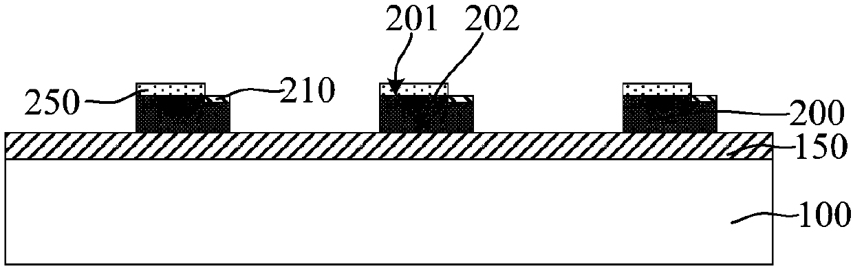
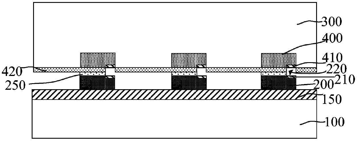
[0033] In order to solve the technical problem, the present invention provides a wafer le...


PUM

PropertyMeasurementUnit
thicknessaaaaaaaaaa
thicknessaaaaaaaaaa

Abstract

The invention provides a wafer level packaging method and a packaging structure. The method comprises the steps: a first wafer is provided, wherein a plurality of first chips are formed in the first wafer, the surface of the first chip is provided with a first electrode, and a first dielectric layer exposing the first electrode is formed on the surface of the first wafer; a plurality of second chips are provided, wherein the surface of the second chip is provided with a second electrode, and a second dielectric layer exposing the second electrode is formed on the second chip; the second dielectric layer and the first dielectric layer are oppositely arranged so that the second chip is enabled to be bonded to the first wafer, wherein the position of the second chip is enabled to correspond to the position of the first chip, and a cavity is formed between the first electrode and the second electrode; a chip interconnection structure for electrically connecting the first electrode and thesecond electrode is formed in the cavity; and a packaging layer covering the second chip is formed. Thus, the packaging process is simplified.

Description

technical field [0001] The invention relates to the technical field of semiconductors, in particular to a wafer-level packaging method and packaging structure. Background technique [0002] With the development trend of very large scale integrated circuits, the feature size of integrated circuits continues to decrease, and people's requirements for packaging technology of integrated circuits continue to increase accordingly. Existing packaging technologies include Ball Grid Array (BGA), Chip Scale Package (CSP), Wafer Level Package (WLP), Three-dimensional Packaging (3D) and System in Package (System in Package, SiP) and so on. [0003] At present, in order to meet the goals of lower cost, more reliability, faster speed and higher density of integrated circuit packaging, the advanced packaging method mainly adopts Wafer Level Package System in Package (WLPSiP). Compared with traditional system packaging, wafer-level system packaging completes the packaging integration proc...

Claims


Application Information

Patent Timeline
Patent Type & Authority Applications(China)
IPC IPC(8): H01L21/56H01L23/31H01L23/528H01L25/16
CPCH01L23/5283H01L23/3114H01L21/56H01L25/165H01L23/528H01L25/16H01L23/31H01L21/02H01L2224/95H01L24/80H01L21/561H01L21/6835H01L23/3121H01L24/08H01L24/92H01L24/94H01L25/0652H01L25/50H01L2221/68354H01L2224/05551H01L2224/08145H01L2224/24145H01L2224/245H01L2224/27505H01L2224/2919H01L2224/29288H01L2224/80006H01L2224/80345H01L2224/80896H01L2224/82101H01L2224/83201H01L2224/8385H01L2224/8389H01L2224/9212H01L2224/94H01L2225/06524H01L2225/06527
Inventor 罗海龙克里夫·德劳利
Owner NINGBO SEMICON INT CORP
Why Eureka
Try Eureka