Liquid ejection head and process for producing liquid ejection head
A liquid ejection head, liquid technology, applied in printing, inking devices, etc., can solve the problem of reducing the positioning accuracy of adjacent chips
- Summary
- Abstract
- Description
- Claims
- Application Information
AI Technical Summary
Problems solved by technology
Method used
Image
Examples
Embodiment 1
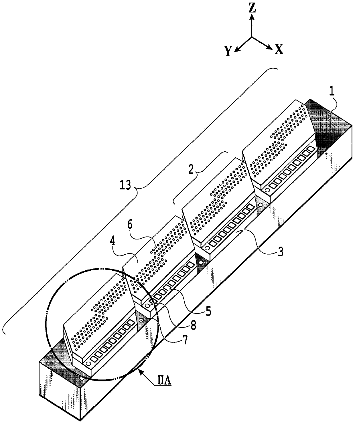
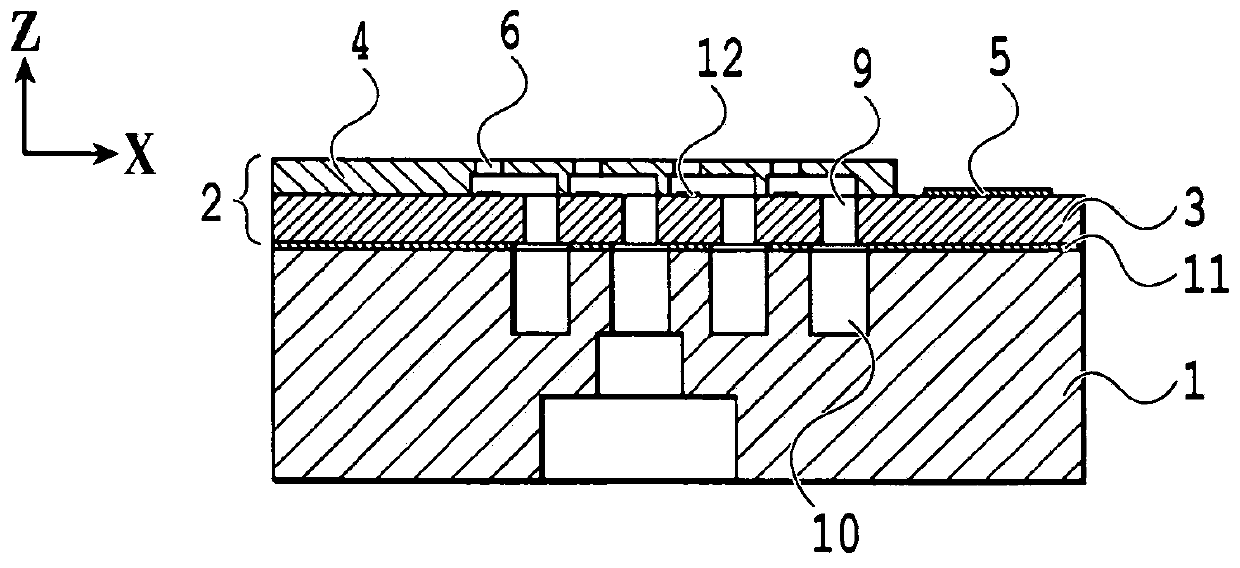
[0015] figure 1 is a perspective view showing an example of the liquid ejection head 13 in this embodiment. The base plate 1 has a liquid flow path structure for supplying liquid (for example, ink) from a tank (not shown) to the device chip 2 . Preferably, the bottom plate 1 should have high chemical and heat resistance, have insulating properties, and should have high mechanical strength. For example, base plate 1 is made of fine ceramics (such as Al 2 o 3 ) and plastics (such as phenolic resin, polycarbonate resin or polyphenylene ether resin).
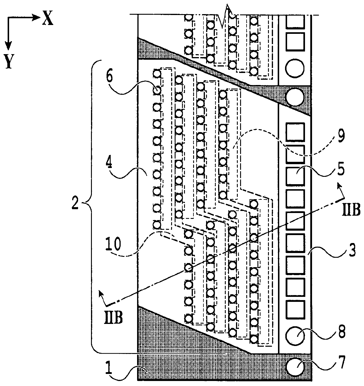
[0016] with adhesive ( figure 1 not shown in ), the device chip 2 is bonded to the upper surface of the base plate 1 in a straight line. figure 1 In the illustrated example, four device chips 2 are arranged, but the number of device chips 2 is not limited to four, and the number of device chips 2 may be any number greater than one. Also, a first reference mark 7 is provided on the upper surface of the bottom plate 1 .
[0017...
Embodiment 2
[0036] In Embodiment 1, a liquid ejection head is described in which device chips are arranged in a line in the printing width direction (Y axis). In Embodiment 2, a liquid ejection head will be described in which device chips are arranged in a matrix in the printing width direction (Y axis) and the direction (X axis) orthogonal to the printing width direction. The manufacturing method is substantially the same as that of Embodiment 1, so the differences will be mainly described below.
[0037] Figure 5 is a view illustrating the device chip in this embodiment. via the binder ( Figure 5 Not shown in ) the device chips 201 to 209 are bonded on the upper surface of the base plate 1 in a matrix form. Figure 5 An example in which nine device chips are arranged on the substrate 1 is shown, but the number of device chips is not limited to nine but may be any number. Each device chip in this embodiment has a shape such that a space is formed between each device chip and each a...
PUM
 Abstract
Description
Claims
Application Information


