Display panel

A display panel and display area technology, applied in static indicators, nonlinear optics, instruments, etc., can solve problems affecting the stability of common electrode wiring and limited space, and achieve the effect of improving stability and large space

Active Publication Date: 2020-03-17
SHENZHEN CHINA STAR OPTOELECTRONICS SEMICON DISPLAY TECH CO LTD
View PDF5 Cites 13 Cited by
  • Summary
  • Abstract
  • Description
  • Claims
  • Application Information

AI Technical Summary

Problems solved by technology

[0005] The present invention provides a display panel, which can solve the problem of the existing display panel. Due to the limited space, the wirin

Method used


Image

  • Display panel
  • Display panel
  • Display panel

Examples


Example Embodiment

[0022] The following descriptions of the various embodiments refer to the accompanying drawings to illustrate specific embodiments in which the invention may be practiced. The directional terms mentioned in the present invention, such as [top], [bottom], [front], [back], [left], [right], [inside], [outside], [side], etc., are only for reference The orientation of the attached schema. Therefore, the directional terms used are used to illustrate and understand the present invention, but not to limit the present invention. In the figures, structurally similar elements are denoted by the same reference numerals.

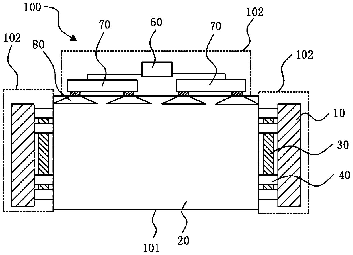
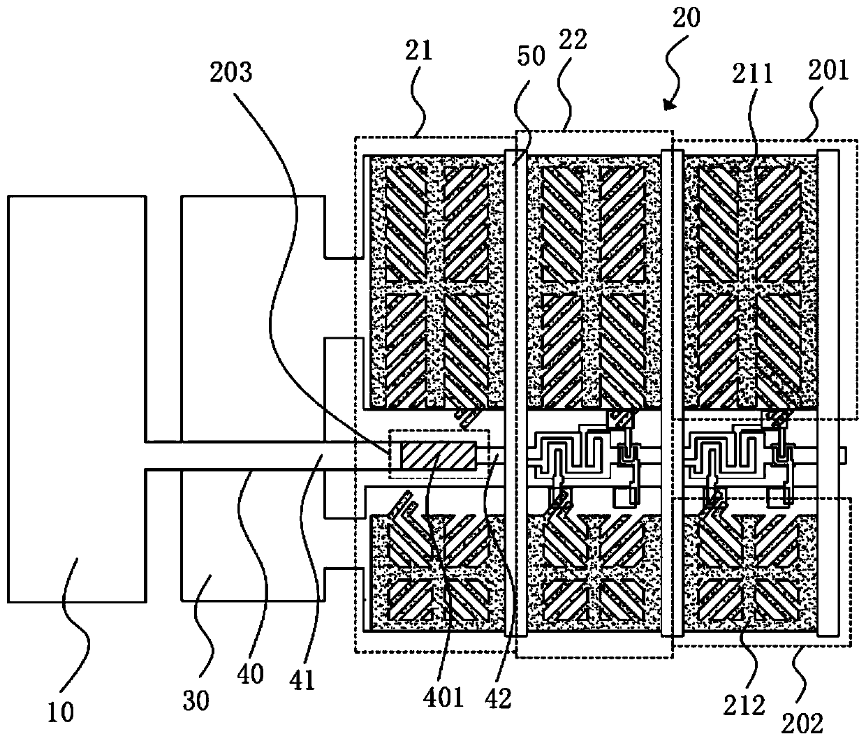
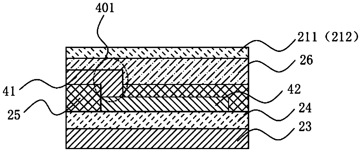
[0023] The present invention aims at the technical problem that the common electrode wiring cannot be designed thick enough due to the limited space of the display panel in the existing display panel, thereby affecting the stability of the common electrode wiring. This embodiment can solve this defect.

[0024] like figure 1 As shown, the embodiment of the present inv...


PUM


Abstract

The invention provides a display panel. The display panel comprises a gate driving circuit, a plurality of pixels, a common electrode signal line and a plurality of scanning lines, wherein a part of the pixels comprise virtual sub-pixels and normal sub-pixels, the virtual sub-pixels are arranged at the periphery of the display area, the common electrode signal lines are located between the gate driving circuit and a display area of the display panel, the scanning lines comprise first scanning signal lines and second scanning signal lines which are arranged on different layers and connected through switching holes, line changing areas are arranged in the virtual sub-pixels, and switching holes are formed in the line changing areas. The display panel is advantaged in that the line changing areas of the scanning lines are arranged in the dotted line pixels, so the scanning lines are changed in the dotted line pixels, original line changing areas can be saved, the common electrode signal lines have larger space, the common electrode signal lines can be thickened, and stability of the common electrode signal lines is improved.

Description

technical field [0001] The present invention relates to the field of display technology, in particular to a display panel. Background technique [0002] Gate Driver On Array, referred to as GOA, realizes the driving mode of progressive scanning of the gate by making the line scanning driving signal circuit on the array substrate by using the array process in the existing thin film transistor liquid crystal display. [0003] In the conventional GOA circuit design, since the output gate trace is the second metal layer trace, if the common electrode trace is also designed as the second metal layer trace, the gate trace will intersect with the common trace, forming Similar to a "T" shape, and the metal on the same layer is prone to ESD (Electro-Static discharge, electrostatic discharge) damage, so in order to avoid the risk of ESD damage, usually, the common electrode wiring uses the first metal layer wiring, so that the gate The wiring crosses the common electrode wiring, and ...

Claims


Application Information

Patent Timeline
IPC IPC(8): G02F1/1362G02F1/1343G09G3/36
CPCG02F1/136286G02F1/1362G02F1/1343G09G3/3674G02F1/13629
Inventor 奚苏萍
Owner SHENZHEN CHINA STAR OPTOELECTRONICS SEMICON DISPLAY TECH CO LTD
Why Eureka
Try Eureka