A bidirectional esd protection device with composite structure

A composite structure and device technology, applied in semiconductor devices, electro-solid devices, electrical components, etc., can solve problems such as high trigger voltage, low sustain voltage, latch-up risk, etc., to reduce trigger voltage, increase sustain voltage, and reduce amplification. multiplier effect

Active Publication Date: 2021-12-03
JIANGNAN UNIV
View PDF0 Cites 0 Cited by
  • Summary
  • Abstract
  • Description
  • Claims
  • Application Information

AI Technical Summary

Problems solved by technology

[0005] For the traditional SCR trigger voltage is too high, the maintenance voltage is too low, and the risk of latch-up is prone to occur

Method used


Image

  • A bidirectional esd protection device with composite structure
  • A bidirectional esd protection device with composite structure
  • A bidirectional esd protection device with composite structure

Examples


Embodiment 1

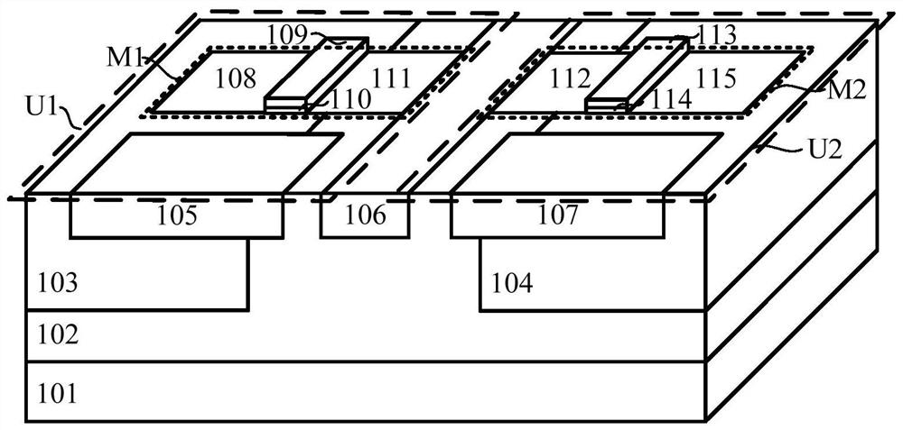
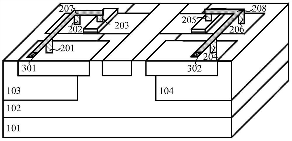
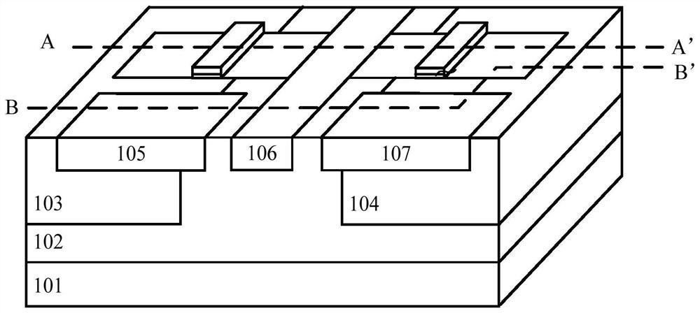
[0032] In this embodiment, a protection device with ESD protection performance is designed, which has a composite structure and layout. Specifically, through a new layout design, the on-state NMOS, the off-state NMOS and the SCR are combined together, and the on-state NMOS and the off-state NMOS are connected in series to form an auxiliary trigger SCR current path to reduce the trigger voltage of the device and increase the P-type The medium doping level increases the base concentration of the parasitic NPN transistor, and the layout design further reduces the emitter area of ​​the parasitic NPN transistor inside the SCR, reduces the magnification of the parasitic transistor inside the SCR, weakens the positive feedback of the SCR, and improves the maintenance of the device Voltage, enhance the voltage clamping ability of the device, expand the stack along the width direction of the device, enhance the robustness of the device, and the completely symmetrical structure enables t...


PUM


Abstract

The invention discloses a bidirectional ESD protection device with a composite structure, which belongs to the fields of electrostatic discharge protection and anti-surge of integrated circuits. The device is mainly composed of a P-type lightly doped substrate, an N-type doped well, a first P-type medium-doped well, a second P-type medium-doped well, a first P-type heavily doped implant region, a first N-type heavily doped implant region, second P-type heavily doped implant region, second N-type heavily doped implant region, first polysilicon gate and its covered first thin gate oxide layer, third N-type heavily doped implant region The doping implantation region, the fourth N-type heavily doped implantation region, the second polysilicon gate and its covered second thin gate oxide layer, and the fifth N-type heavily doped implantation region. The present invention improves the base concentration of the parasitic NPN transistor inside the device through the layout design and the use of the P-type doped well, reduces the magnification of the internal parasitic NPN transistor, weakens the positive feedback degree of the parasitic SCR structure, and can increase the maintenance voltage of the device and enhance ESD robustness.

Description

technical field [0001] The invention relates to a bidirectional ESD protection device with a composite structure, which belongs to the field of electrostatic discharge protection and anti-surge of integrated circuits. Background technique [0002] The surge phenomenon of electronic products refers to the peak current or voltage that is much larger than the steady state generated by the circuit at the moment of power-on or when an abnormal situation occurs. The essence is a violent pulse generated in a very short time. Because the surge occurs for a very short time, and the magnitude of the surge voltage or current is much greater than the steady-state voltage and current, the damage caused by the surge to devices, circuits and electronic products cannot be ignored. There are many sources of surges, and electrostatic discharge is one of the main ones. Electrostatic discharge refers to the charge transfer caused by objects with different electrostatic potentials approaching e...

Claims


Application Information

Patent Timeline
Patent Type & Authority Patents(China)
IPC IPC(8): H01L27/02H01L29/06
CPCH01L27/0266H01L29/0603H01L29/0684
Inventor 梁海莲朱玲顾晓峰虞致国姜岩峰闫大为
Owner JIANGNAN UNIV
Why Eureka
Try Eureka