

Display device
A display device and waveguide layer technology, applied in optical components, optics, instruments, etc., can solve the problem of low light energy utilization rate, achieve the effects of reducing light leakage, improving performance and user experience, and improving light energy utilization rate
- Summary
- Abstract
- Description
- Claims
- Application Information
AI Technical Summary
Problems solved by technology
Method used
Image

Examples
Embodiment Construction
[0037] In order to enable those skilled in the art to better understand the technical solutions in the present invention, the technical solutions in the embodiments of the present invention will be clearly and completely described below in conjunction with the drawings in the embodiments of the present invention. Obviously, the described The embodiments are only some of the embodiments of the present invention, not all of them. Based on the embodiments of the present invention, all other embodiments obtained by persons of ordinary skill in the art without making creative efforts shall fall within the protection scope of the present invention.
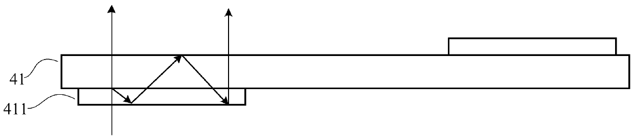
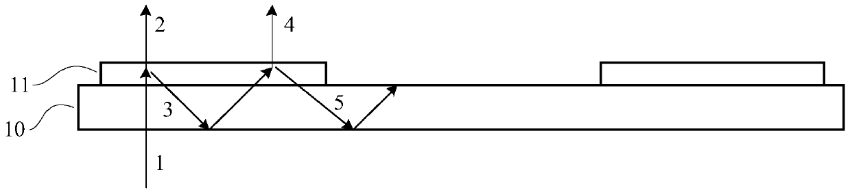
[0038] Please refer to figure 1 , figure 1 It is a schematic diagram of the optical path of an existing waveguide-based display device, assuming that the diffraction efficiency of the coupling element 11 is 30%, and without considering absorption, the energy of the incident light 1 is 100%, and the light 2 is the zero-order output of t...
PUM
 Abstract
Description
Claims
Application Information