Photosensitive circuit, method for preparing photosensitive circuit, and display device

A circuit and semiconductor technology, applied in the fields of photosensitive circuits, photosensitive circuit preparation methods, and display devices, can solve the problems of low light sensitivity of photosensitive circuits, and achieve good threshold voltage stability, low threshold voltage stability, and high electron migration rate effect

Active Publication Date: 2022-03-29
SHENZHEN ROYOLE TECH CO LTD
View PDF4 Cites 0 Cited by
  • Summary
  • Abstract
  • Description
  • Claims
  • Application Information

AI Technical Summary

Problems solved by technology

However, when the thin film transistor is applied to the photosensitive circuit, it will cause the problem that the light sensitivity of the photosensitive circuit is not strong.

Method used


Image

  • Photosensitive circuit, method for preparing photosensitive circuit, and display device
  • Photosensitive circuit, method for preparing photosensitive circuit, and display device
  • Photosensitive circuit, method for preparing photosensitive circuit, and display device

Examples


Embodiment Construction

[0022] The following will clearly and completely describe the technical solutions in the embodiments of the present invention with reference to the accompanying drawings in the embodiments of the present invention. Obviously, the described embodiments are only some, not all, embodiments of the present invention. Based on the embodiments of the present invention, all other embodiments obtained by persons of ordinary skill in the art without making creative efforts belong to the protection scope of the present invention.

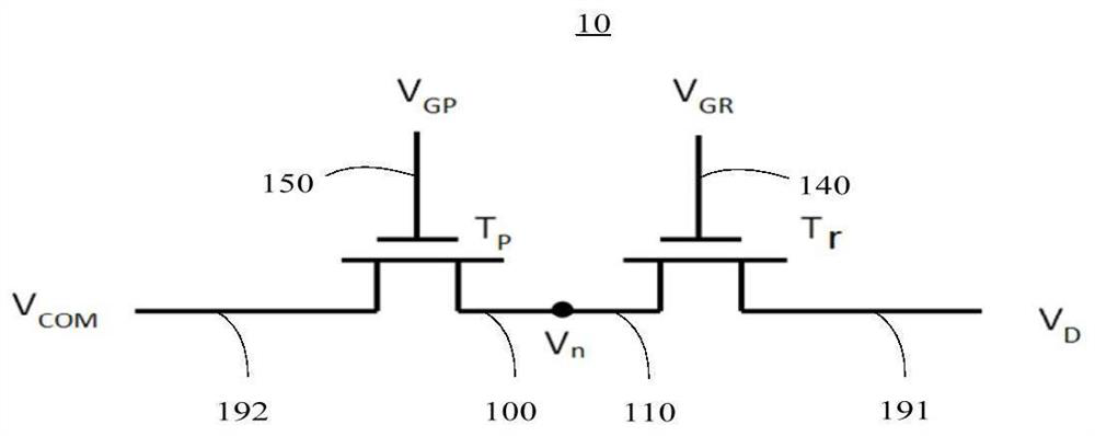
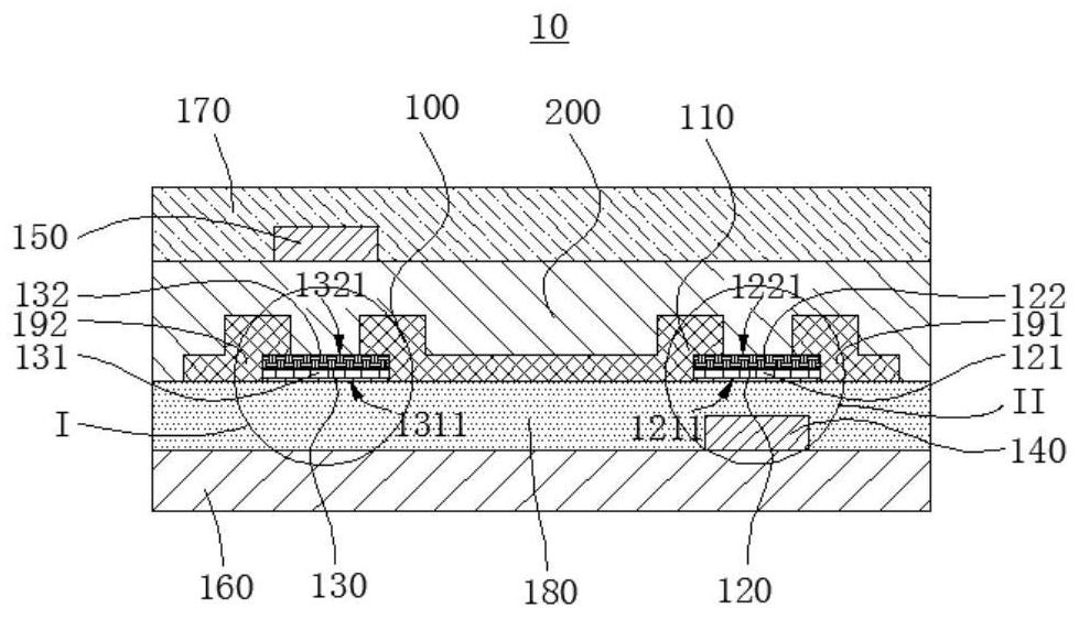
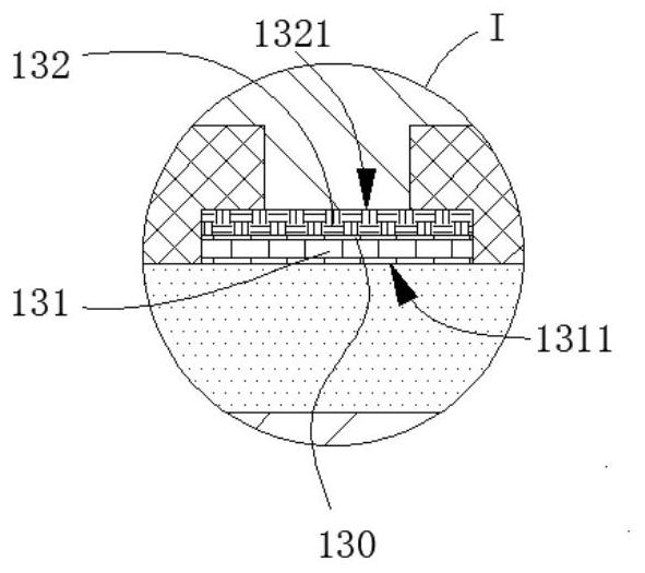
[0023] see figure 1 , figure 2 , image 3 and Figure 4 , figure 1 It is a schematic diagram of the circuit structure of the photosensitive circuit provided by the present invention. figure 2 It is a schematic structural diagram of the photosensitive circuit of Embodiment 1 of the present invention. image 3 It is an enlarged schematic diagram of part I of the photosensitive circuit according to Embodiment 1 of the present invention. Figure 4 It is an...


PUM


Abstract

A photosensitive circuit (10), a method for preparing the photosensitive circuit (10), and a display device. The photosensitive circuit (10) includes a first thin film transistor (Tr) and a second thin film transistor (Tp), the drain (100) of the second thin film transistor is electrically connected to the source (110, 191) of the first thin film transistor, and the first thin film transistor The transistor includes a first active layer (120), the second thin film transistor includes a second active layer (130), the first active layer (120) includes a first semiconductor portion (121), and the second active layer (130) It includes a second semiconductor portion (131), the first and second semiconductor portions (131) are arranged in the same layer and spaced apart, the first active layer (120) includes a third semiconductor portion (122), and the third semiconductor portion (122) is arranged On the first semiconductor portion (121), the second active layer (130) includes a fourth semiconductor portion (132), the fourth semiconductor portion (132) is arranged on the second semiconductor portion (131), the third and fourth The semiconductor parts (132) are arranged on the same layer at intervals, the first semiconductor part (121) is adjacent to the gate (140) of the first thin film transistor, the fourth semiconductor part (132) is adjacent to the gate (150) of the second thin film transistor, and the second semiconductor part (132) is adjacent to the gate (150) of the second thin film transistor. The defect state density of the third semiconductor portion (122) is higher than the defect state density of the first semiconductor portion (121), and the defect state density of the fourth semiconductor portion (132) is higher than the defect state density of the second semiconductor portion (131) density of.

Description

technical field [0001] The invention relates to the field of photosensitive circuits, in particular to a photosensitive circuit, a method for preparing the photosensitive circuit and a display device. Background technique [0002] In recent years, thin film transistors have received more and more attention because of their advantages such as high mobility, good light transmission, stable film structure, low preparation temperature and low cost. The main goal of the development of thin film transistors is to be used in flat panel displays, flexible electronic devices, transparent electronic devices, liquid crystal displays, organic light-emitting diodes, and sensors. However, when the thin film transistor is applied to a photosensitive circuit, the light sensitivity of the photosensitive circuit is not strong. Contents of the invention [0003] An embodiment of the present invention provides a photosensitive circuit. The photosensitive circuit includes a first thin film t...

Claims


Application Information

Patent Timeline
Patent Type & Authority Patents(China)
IPC IPC(8): G02F1/1368G09F9/30
CPCG02F1/1368G09F9/30
Inventor 陈小明赵云飞李明亮刘佳豪
Owner SHENZHEN ROYOLE TECH CO LTD
Why Eureka
Try Eureka