

Signal acquisition device, signal acquisition method, display device and electronic equipment
Patent Information
- Authority / Receiving Office
- CN · China
- Current Assignee / Owner
- CHIPONE TECH BEIJINGCO LTD
- Publication Date
- 2020-03-27
Smart Images
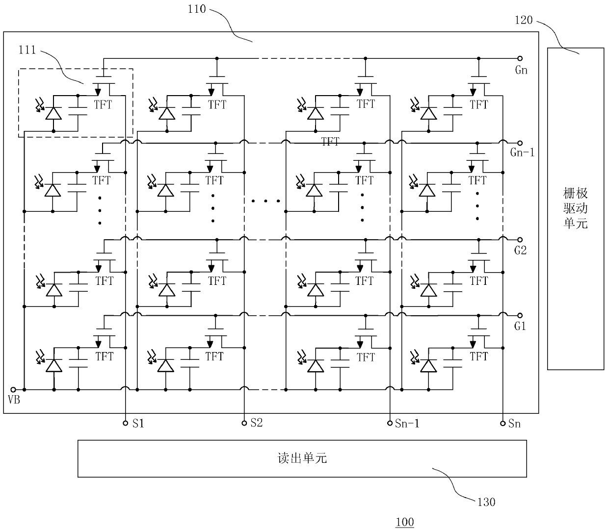
Figure 1 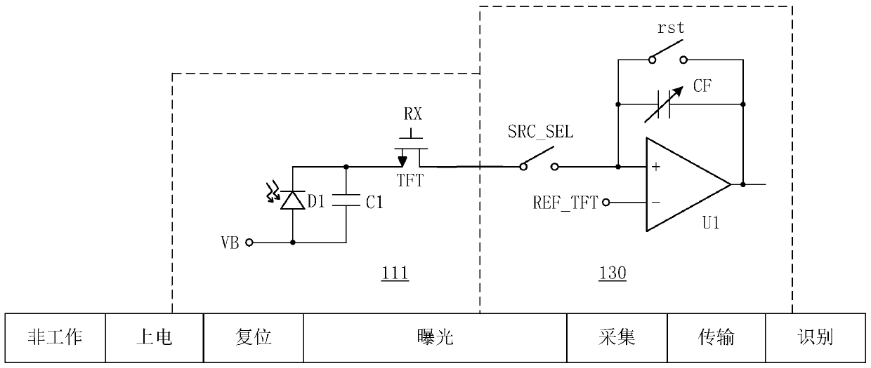
Figure 2 
Figure 3
Abstract
Description
technical field
[0001] The present invention relates to the field of optical touch technology, in particular to a signal collection device, a collection method, a display device and electronic equipment. Background technique
[0002] In OLED (Organic Light-Emitting Diode, Organic Light-Emitting Diode) screens, the capacitive touch chip needs to use the sensor on the panel to complete the touch control, while the full-screen optical fingerprint recognition requires another layer of photodiode sensor array to complete the fingerprint recognition. identify.
[0003] Optical fingerprint recognition usually uses the screen of the terminal device as the light-emitting body, irradiates the fingerprint through the optical path, and the returned light passes through the screen and returns to the image sensor under the screen. The terminal device analyzes and compares the returned image with the database to finally identify the fingerprint. Optical fingerprint recognition uses the pr...