Display panel and display device

A display panel and display unit technology, applied in identification devices, circuit devices, static indicators, etc., can solve problems such as high product cost and signal interference, and achieve the effects of improved performance, good uniformity, and reduced attenuation

Pending Publication Date: 2020-04-10
BOE TECH GRP CO LTD +1
View PDF0 Cites 8 Cited by
  • Summary
  • Abstract
  • Description
  • Claims
  • Application Information

AI Technical Summary

Problems solved by technology

[0004] The purpose of this disclosure is to overcome the problems of easy signal interference and high product cost in related technologies, and provide a display panel that can shield signal electromagnetic interference, improve performance, and can replace wave-absorbing materials , thus reducing the cost

Method used


Image

  • Display panel and display device
  • Display panel and display device
  • Display panel and display device

Examples


Embodiment 1

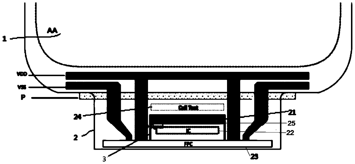
[0041] Such as figure 1 As shown, in Embodiment 1 of the present disclosure, the multiplexer 21 is disposed below the bending position P and adjacent to the IC chip 22 . By arranging the multiplexer 21 below the bending position P, it is folded to the back of the panel after being bent, so that the size design is relatively compact and the proportion of the screen is relatively large. In addition, disposing the multiplexer 21 adjacent to the IC chip 22 can reduce interference during signal transmission, reduce output impedance, reduce signal attenuation, and improve signal clarity.

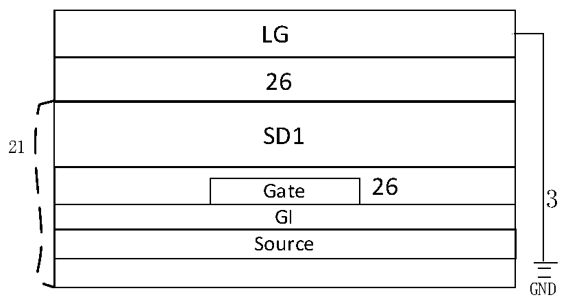
[0042] The multiplexer 21 is composed of the first source-drain metal layer SD1, etc.; the structure of the first source-drain metal layer SD1 is Ti-Al-Ti; it has good conductivity and low impedance; it can reduce the signal transmission process Power consumption in reducing signal attenuation; Multiplexer 21 also includes active layer source and gate layer gate, there is gate insulating layer GI...

Embodiment 2

[0049] Such as figure 1 As shown, in Embodiment 2 of the present disclosure, the multiplexer 21 is arranged below the bending position P, adjacent to the position of the IC chip 22; the multiplexer 21 includes a surface-covered first source-drain metal layer SD1; The path selector SD1 also includes an active layer source and a gate layer gate. There is a gate insulating layer GI between the active layer source and the gate layer gate. The first source-drain metal layer SD1 is connected to the active layer source gate. connect.

[0050] The structure of the first source-drain metal layer SD1 is Ti-Al-Ti; the first source-drain metal layer SD1 runs through the entire display panel as a signal line, including Data data signal line, Goa signal line, internal working voltage VDD signal line or the common ground voltage VSS signal line; the first source-drain metal layer SD1 is covered with a passivation layer and a flat layer as the first insulating layer 26; the first insulating ...

Embodiment 3

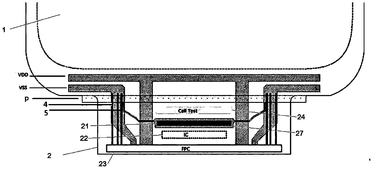
[0058] Such as figure 2 As shown, Embodiment 3 of the present disclosure includes a multi-layer flexible metal layer disposed on the flexible substrate and capable of conducting signals, and the multi-layer flexible metal layer includes at least one touch sensor connected to the FMLOC touch ground terminal 5 The metal layer 27 , the metal shielding layer 25 is a part of the at least one touch metal layer 27 . The formation method of at least one touch metal layer 27 in this embodiment is suitable for a bendable display panel product with a single source and drain metal layer and a FMLOC flexible metal layer, and the specific structure is as follows:

[0059] As mentioned above, the multiplexer 21 is arranged below the bending position P, adjacent to the position of the IC chip 22; the multiplexer 21 includes the first source-drain metal layer SD1; the first source-drain metal layer The structure of layer SD1 is Ti-Al-Ti; the first source-drain metal layer SD1 runs through th...


PUM


Abstract

The invention provides a display panel and a display device. The display panel comprises a flexible substrate, the flexible substrate comprises a display unit and a bending unit which is connected with the display unit and can be bent to the back face of the display unit. The bending unit comprises a multiplexer, a chip and a flexible circuit board which are sequentially arranged in the downward direction away from the bending position. The flexible circuit board comprises a grounding end capable of providing a grounding signal, the surface, away from the flexible substrate, of the multiplexeris provided with a metal shielding layer and an insulating layer which is arranged between the metal shielding layer and the multiplexer and used for insulation and isolation, and the metal shieldinglayer is connected with the grounding end to shield signal interference. According to the display panel and the display device provided by the invention, electromagnetic signal interference can be shielded, the use performance is improved, and the wave-absorbing material is reduced or not coated, so that the cost is reduced.

Description

technical field [0001] The present disclosure relates to the display field, and in particular to a display panel and a display device. Background technique [0002] With the development of the display industry, the full screen has gradually become the trend. The panel technology is designed by COF (Chip On Flex or Chip On Film, often called chip-on-chip film, which fixes the driver IC chip on the flexible circuit board. , which uses a flexible additional circuit board as a chip carrier to package the chip, and the technology of bonding the chip to the flexible substrate circuit) gradually shifts to COP design (Chip On Pi, the backplane of the flexible OLED screen is not the unique glass of LCD, and the materials used and Similar to the FPC soft board, it is flexible and can be curled at will. Therefore, the screen of the COP package can be directly folded back on the basis of the COF, thereby minimizing the occupation of the "chin" space by the screen module), which can Eff...

Claims


Application Information

Patent Timeline
Patent Type & Authority Applications(China)
IPC IPC(8): G09F9/30H05K9/00
CPCG09F9/301G09F9/33H05K9/0054G09G2330/06G09G2310/0297G09G3/3208H05K2201/10128H05K1/189H05K1/0218H10K59/12H10K71/70G09G3/006H10K50/84H10K59/40H10K59/126H10K59/131
Inventor 都蒙蒙董向丹马宏伟颜俊程博
Owner BOE TECH GRP CO LTD
Why Eureka
Try Eureka