Chip stacking and packaging method and packaging structure
A technology of chip stacking and packaging methods, which is applied in the manufacture of electrical components, electrical solid devices, semiconductor/solid devices, etc., and can solve the problems of low production yield of chip packaging structures, increased preparation costs of chip stacking packaging structures, and many unqualified finished products, etc. problem, to achieve the effect of reducing implementation difficulty, high yield, and reducing production cost
- Summary
- Abstract
- Description
- Claims
- Application Information
AI Technical Summary
Problems solved by technology
Method used
Image
Examples
Embodiment 1
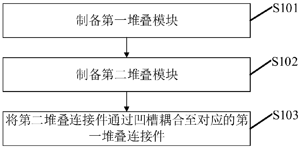
[0039] This embodiment provides a fan-out chip stack packaging method, such as figure 1 As shown, the packaging structure method includes the following steps:
[0040] S101: Prepare the first stacking module 1 .
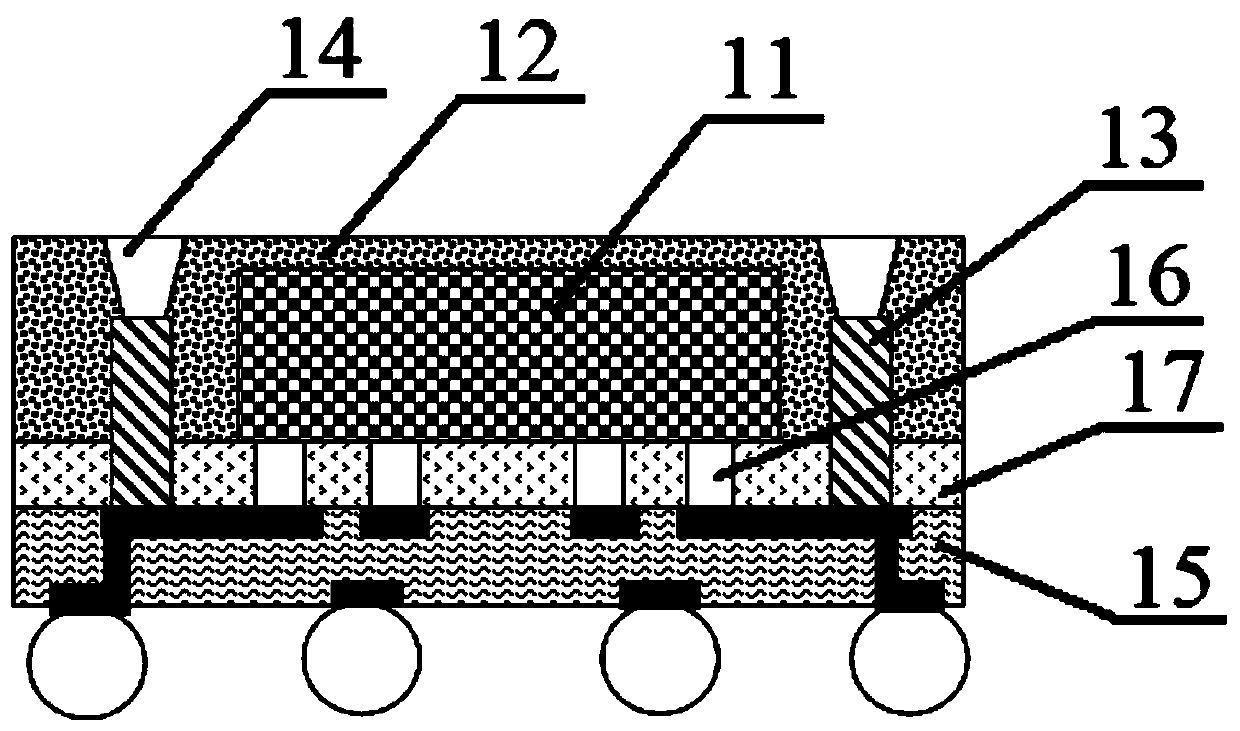
[0041] here, as figure 2 As shown, the first stack module 1 includes a first chip 11, a first package body 12 and a first stack connector 13, wherein the first package body 12 encapsulates the first chip 11, and the first stack connector 13 is also arranged on In the first package 12, one end of the first stack connector 13 is coupled to the first chip 11, and the other end is exposed to the first package through a groove 14 corresponding to the first stack connector 13 in the first package. A package body 12 outside.
[0042] Here, the first chip 11 is a general term for all the chips in the first stacked module 1, specifically, the first chip 11 can be one chip or multiple chips, and when the first chip 11 is multiple chips, The plurality of chips may be of th...
Embodiment 2
[0089] This embodiment provides a chip stack packaging structure, and the chip stack packaging structure can be prepared according to the chip stack packaging method and its preferred implementation in Embodiment 1, and what has already been described will not be repeated.
[0090] The chip stack package structure provided by the embodiment of the present invention, such as Figure 4 As shown, it includes: a first stacking module 1 and a second stacking module 2 .
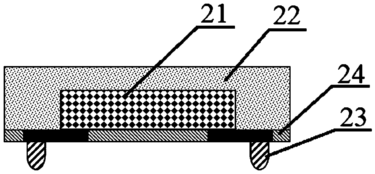
[0091] Wherein, the first stack module 1 includes a first chip 11 , a first package body 12 and a first stack connector 13 . Specifically, the first package 12 encapsulates the first chip 11, and one end of the first stack connector 13 is coupled to the first chip 11, and the other end is connected to the first stack connector 13 through the first package. The corresponding groove 14 is exposed outside the first package body 12 . The second stack module 2 includes a second chip 21, a second package body 22 and a ...
PUM
 Abstract
Description
Claims
Application Information
 - R&D
- Intellectual Property
- Life Sciences
- Materials
- Tech Scout
- Unparalleled Data Quality
- Higher Quality Content
- 60% Fewer Hallucinations
Browse by: Latest US Patents, China's latest patents, Technical Efficacy Thesaurus, Application Domain, Technology Topic, Popular Technical Reports.
© 2025 PatSnap. All rights reserved.Legal|Privacy policy|Modern Slavery Act Transparency Statement|Sitemap|About US| Contact US: help@patsnap.com


