Test chip and integration method

An integration method and chip technology, applied in the direction of electronic circuit testing, measuring electricity, measuring devices, etc., can solve the problems of chip/electronic device failure, open circuit, etc., and achieve the effect of improving reliability, life, and high flexibility

Pending Publication Date: 2020-04-14
苏州容启传感器科技有限公司
View PDF9 Cites 3 Cited by
  • Summary
  • Abstract
  • Description
  • Claims
  • Application Information

AI Technical Summary

Problems solved by technology

When the electronic device is working, driven by the electric field of direct current, the electrons move from the negative pole to the positive pole of the conductor, and its kinetic energy also promotes the movement of metal atoms from t

Method used


Image

  • Test chip and integration method
  • Test chip and integration method
  • Test chip and integration method

Examples


Embodiment Construction

[0060] The specific implementation manners according to the present invention will be described below in conjunction with the accompanying drawings.

[0061] In the following description, many specific details are set forth in order to fully understand the present invention, but the present invention can also be implemented in other ways different from those described here, therefore, the present invention is not limited to the specific embodiments disclosed below limit.

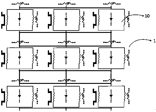
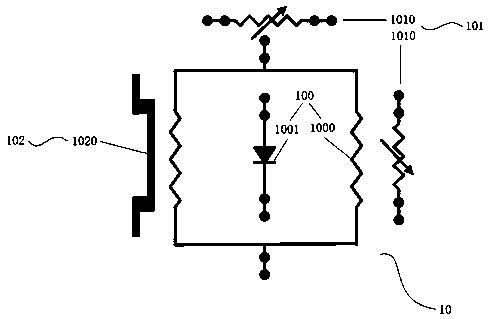
[0062] The present invention provides a test chip, for details see Figure 1 to Figure 3 , including a test unit 1, the test unit 1 is distributed in a chip (not shown in the figure) singly or in an array, the test unit 1 includes a number of basic units 10 distributed in an array, and several basic units 10 have the functions of series, parallel or both series and Parallel connection relationship; each basic unit 10 includes a thermal test module 100, a stress test module 101 and an electromigration test m...


PUM


Abstract

The invention provides a test chip which comprises test units, the test units are distributed in the chip in a single or array mode, each test unit comprises a plurality of basic units distributed inan array mode, and the basic units are connected in series, in parallel or both in series and in parallel. Each basic unit comprises a thermal test module, a stress test module and an electromigrationtest module; wherein the thermal test module comprises a heating element and a temperature measuring element; the stress test module comprises a stress test element; the electromigration test modulecomprises an electromigration test element; and the heating element, the temperature measuring element, the stress testing element and the electromigration testing element are externally connected with a driving power supply and a signal reading circuit respectively. The invention also provides an integration method of the test chip.

Description

technical field [0001] The invention relates to the technical field of semiconductor microfabrication, in particular to a test chip and an integration method. Background technique [0002] The reduction of transistor feature size and the advancement of three-dimensional packaging technology have promoted the continuous development of electronic devices in the direction of smaller feature size and high integration. Therefore, whether in the plane or in the three-dimensional direction, the transistor density and integration of electronic components are constantly increasing. The transmission and movement performance of the internal carriers in the channel changes. When the temperature of this point exceeds its normal operating temperature range, the chip performance will deviate from the normal working state, or even fail, especially for high-power, high-frequency devices, which are caused by chip heating. The problem is even worse. [0003] Therefore, the temperature distri...

Claims


Application Information

Patent Timeline
IPC IPC(8): G01R31/28
CPCG01R31/2874G01R31/2879G01R31/2881G01R31/2898
Inventor 王媛
Owner 苏州容启传感器科技有限公司
Why Eureka
Try Eureka