Three-dimensional photonic crystal and its application

A photonic crystal, three-dimensional technology, applied in optics, optical components, instruments, etc., can solve the problem of photonic band gap limitation, inability to form an effective band gap, and high incidence angle dependence.

Active Publication Date: 2021-08-10
SHENZHEN HOLOKOOK TECH CO LTD
View PDF8 Cites 0 Cited by
  • Summary
  • Abstract
  • Description
  • Claims
  • Application Information

AI Technical Summary

Problems solved by technology

[0004] However, since the photonic bandgap of two-dimensional photonic crystals is limited to two-dimensional space, an effective forbidden band cannot be formed in three-dimensional space. The incident light wave of two-dimensional photonic crystals has an out-of-plane wave vector, which needs to rely on the interface between the flat medium and the air medium. Total reflection is used to constrain the propagation of light waves in the two-dimensional photonic crystal plane wave, that is, the two-dimensional photonic crystal is more sensitive to the incident angle of the input optical signal (high dependence)

Method used


Image

  • Three-dimensional photonic crystal and its application
  • Three-dimensional photonic crystal and its application
  • Three-dimensional photonic crystal and its application

Examples


Embodiment 1

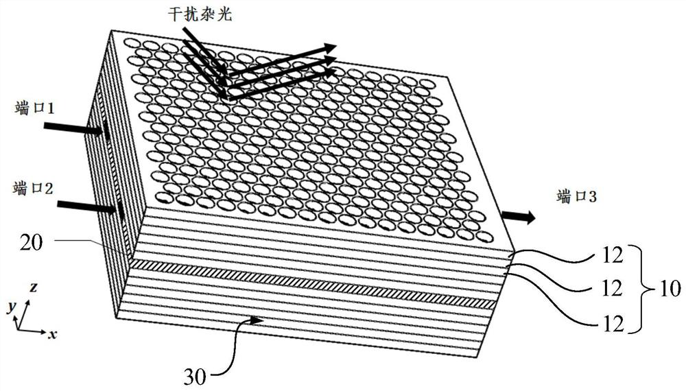
[0058] This example is prepared as figure 1 The 3D photonic crystal shown.

[0059] Through electron beam exposure combined with reactive ion beam etching technology, an array of holes arranged periodically in a triangular hexagonal structure is etched on the SOI wafer to obtain a base layer. Wherein, the distance between two adjacent holes is recorded as a, and the wavelength λ of the input optical signal is 1550nm, so it can be obtained that a=738nm, the aperture size is 0.88a, and the thickness of the SOI wafer is 0.82a.

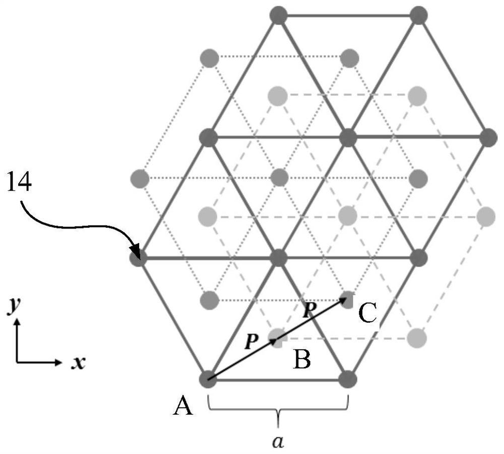
[0060] When the three base layers are stacked together by wafer bonding technology, and when the hole array is etched on each silicon monolayer, the position of the hole array is relative to the upper layer, and there is one on the xy plane. image 3 The displacement along the vector P(0.5a, 0.29a) is shown, thus obtaining a periodic structure.

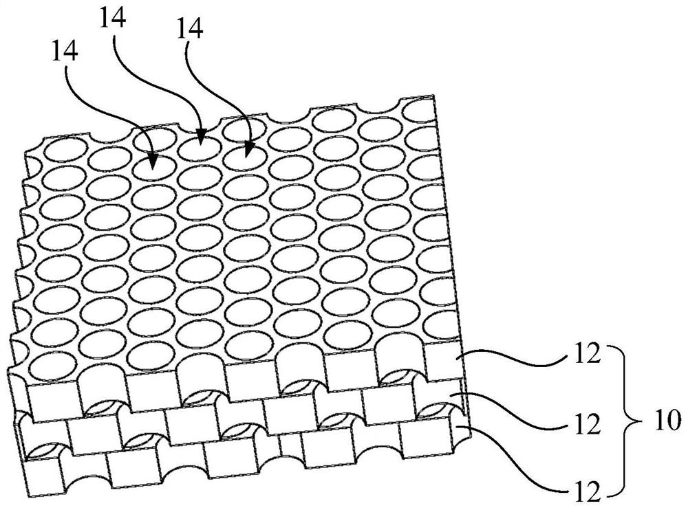
[0061] to combine Figure 4 , in the process of preparing the base layer, after selectively removing 5 rows...


PUM


Abstract

The invention relates to a three-dimensional photonic crystal and its application in the field of optical devices. The three-dimensional photonic crystal includes a first periodic layer, a defect layer, and a second periodic layer stacked in sequence; the number of periods of the first periodic layer is at least 2, and the first periodic layer includes at least 2 base layers that are sequentially dislocated and stacked together, each A number of evenly distributed through-holes are provided on each base layer. In each base layer, the distance between two adjacent through-holes is equal and denoted as a; the defective layer is the base layer where line defects are introduced; the second periodic layer’s Both the structure and the number of periods are the same as the first period layer. The above-mentioned three-dimensional photonic crystal forms periodic changes through multi-layer dislocation stacking in space through the base layer of the two-dimensional structure, so that the three-dimensional photonic crystal has a complete photonic band gap, which can limit the propagation of optical signals of specific wavelength bands in three-dimensional space. This 3D photonic crystal is insensitive to the angle of incidence of the incoming signal.

Description

technical field [0001] The invention relates to the field of optical path adjustment devices, in particular to a three-dimensional photonic crystal and its application. Background technique [0002] A photonic crystal is a material structure in which dielectric materials are periodically arranged in space, and is usually an artificial crystal composed of two or more materials with different dielectric constants. Photonic crystals have a strong and flexible ability to control the propagation of light. The introduction of point defects in the photonic crystal structure can build optical resonant microcavities, or introduce line defects to create photonic crystal optical waveguides. Optical resonators and optical waveguide structures based on photonic crystal point defects and line defects can be used to construct optical switches, optical operation logic devices, and micro-laser resonators, and have the advantages of miniaturization and integration, and can adapt to future te...

Claims


Application Information

Patent Timeline
Patent Type & Authority Patents(China)
IPC IPC(8): G02B1/00
CPCG02B1/005
Inventor 郭滨刚
Owner SHENZHEN HOLOKOOK TECH CO LTD
Why Eureka
Try Eureka