Bulk acoustic wave resonator with electrical isolation layer, manufacturing method of bulk acoustic wave resonator, filter and electronic equipment

A bulk acoustic wave resonator and isolation layer technology, applied in the field of bulk acoustic wave resonator and bulk acoustic wave resonator manufacturing, can solve the problem of increasing process difficulty, wafer-level device packaging complexity, reduction of electromechanical coupling coefficient, growth of single crystal materials, etc. question

Active Publication Date: 2020-04-17
ROFS MICROSYST TIANJIN CO LTD
View PDF12 Cites 7 Cited by
  • Summary
  • Abstract
  • Description
  • Claims
  • Application Information

AI Technical Summary

Problems solved by technology

[0004] In traditional bulk acoustic wave resonators, the bottom-up processing method is often used. The key step is to pattern the bottom electrode after sputtering the bottom electrode and then continue to grow the piezoelectric layer, resulting in the piezoelectric layer on the electrode. The edge is prone to breakage or crystal orientation changes, resulting in a decrease in the electromechanical coupling coefficient
[0005] In addition, in single crystal acoustic resonators, since single crystal growth has extremely high requirements on interface materials, interface crystallinity, interface cleanliness, roughness, and flatness, it is not possible to grow single crystal materials directly on the patterned bottom electrode. , the method of back etching is often used to deposit the bottom electrode, which increases the difficulty of the process and the complexity of wafer-level device packaging (both sides of the front and back are required)

Method used


Image

  • Bulk acoustic wave resonator with electrical isolation layer, manufacturing method of bulk acoustic wave resonator, filter and electronic equipment
  • Bulk acoustic wave resonator with electrical isolation layer, manufacturing method of bulk acoustic wave resonator, filter and electronic equipment
  • Bulk acoustic wave resonator with electrical isolation layer, manufacturing method of bulk acoustic wave resonator, filter and electronic equipment

Examples


Embodiment Construction

[0032] The technical solutions of the present invention will be further specifically described below through the embodiments and in conjunction with the accompanying drawings. In the specification, the same or similar reference numerals designate the same or similar components. The following description of the embodiments of the present invention with reference to the accompanying drawings is intended to explain the general inventive concept of the present invention, but should not be construed as a limitation of the present invention.

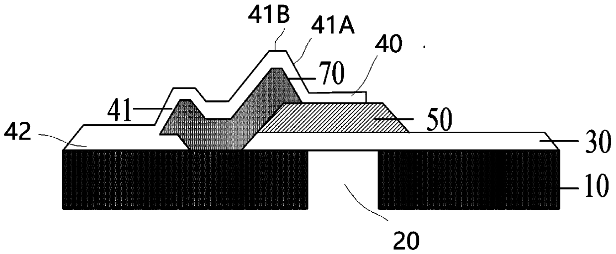
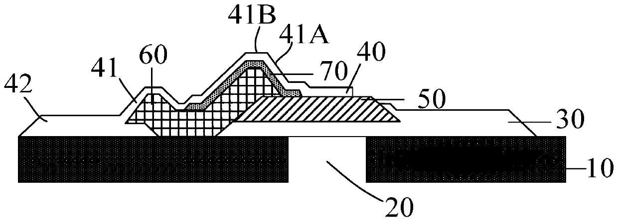
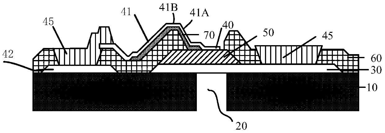
[0033] In the present invention, a bulk acoustic wave resonator is prepared on a single crystal piezoelectric layer with a bottom electrode obtained by directly growing a piezoelectric layer after growing the bottom electrode or by other methods (such as bonding) through a top-down processing method. , leading out the top electrode by adding an air or dielectric isolation layer. The invention can also minimize the parasitic capacitance betwee...


PUM


Abstract

The invention discloses a bulk acoustic wave resonator. The bulk acoustic wave resonator comprises a substrate, a bottom electrode, a top electrode, a piezoelectric layer disposed between the bottom electrode and the top electrode and an acoustic mirror. The resonator further comprises an electrode connecting part, an electrical isolation layer and an electrode pin; the electrode connecting part covers the electrical isolation layer, one end of the electrode connecting part is electrically connected with the top electrode, and the other end of the electrode connecting part is suitable for being electrically connected with the electrode pin; one part of the electrical isolation layer forms electrical isolation between the electrode connecting part of the resonator and the bottom electrode;and at least one part of the electrical isolation layer covers at least one part of the end surface of the piezoelectric layer and the end surface of the bottom electrode so as to form electrical isolation between the electrode connecting part and the bottom electrode. The invention further discloses a manufacturing method of the bulk acoustic wave resonator, a filter with the resonator and electronic equipment with the filter or the resonator.

Description

technical field [0001] The invention relates to the field of semiconductors, in particular to a bulk acoustic wave resonator, a filter, an electronic device with the resonator or the filter, and a manufacturing method of the bulk acoustic wave resonator. Background technique [0002] As the basic elements of electronic equipment, electronic devices have been widely used, including mobile phones, automobiles, home appliances, etc. In addition, technologies such as artificial intelligence, the Internet of Things, and 5G communications that will change the world in the future still need to rely on electronic devices as the basis. [0003] Film Bulk Acoustic Resonator (FBAR, also known as Bulk Acoustic Resonator, also known as BAW), as an important member of piezoelectric devices, is playing an important role in the field of communication, especially FBAR filters in radio frequency filters The field market share is increasing. FBAR has excellent characteristics such as small si...

Claims


Application Information

Patent Timeline
Patent Type & Authority Applications(China)
IPC IPC(8): H03H9/15H03H9/17H03H9/13
CPCH03H9/15H03H9/17H03H9/13H03H2009/02503H03H2009/155H03H9/132H03H9/02118H03H3/02H03H9/02125H03H9/171H03H9/02133
Inventor 庞慰杨清瑞张孟伦
Owner ROFS MICROSYST TIANJIN CO LTD
Why Eureka
Try Eureka