Light-emitting diode epitaxial wafer and preparation method thereof

A technology of light-emitting diodes and epitaxial wafers, applied in electrical components, circuits, semiconductor devices, etc., can solve the problems of decreased luminous efficiency, red shift of luminous peaks, unsatisfactory luminous efficiency of InGaN/GaN multiple quantum well layers, etc. Polarization effect, the effect of improving the luminous effect

Active Publication Date: 2020-04-21
HC SEMITEK SUZHOU
View PDF6 Cites 7 Cited by
  • Summary
  • Abstract
  • Description
  • Claims
  • Application Information

AI Technical Summary

Problems solved by technology

Due to the existence of piezoelectric polarization and spontaneous polarization in the InGaN / GaN multi-quantum well layer, piezoelectric polarization and spontaneous polarization will cause the quantum confinement Stark effect, that is, piezoelectric polarization and spontaneous polarization lead to electron-hole For the phenomena of spatial separation and reduction of wave function overlap, the luminous efficiency of InGaN / GaN multi-quantum well layer decreases, and the luminous peak (absorption edge) red shifts
The luminous efficiency of the resulting InGaN / GaN multi-quantum well layer is still not ideal

Method used


Image

  • Light-emitting diode epitaxial wafer and preparation method thereof
  • Light-emitting diode epitaxial wafer and preparation method thereof
  • Light-emitting diode epitaxial wafer and preparation method thereof

Examples


Embodiment Construction

[0027] In order to make the purpose, technical solution and advantages of the present disclosure clearer, the implementation manners of the present disclosure will be further described in detail below in conjunction with the accompanying drawings.

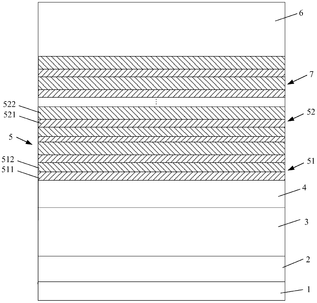
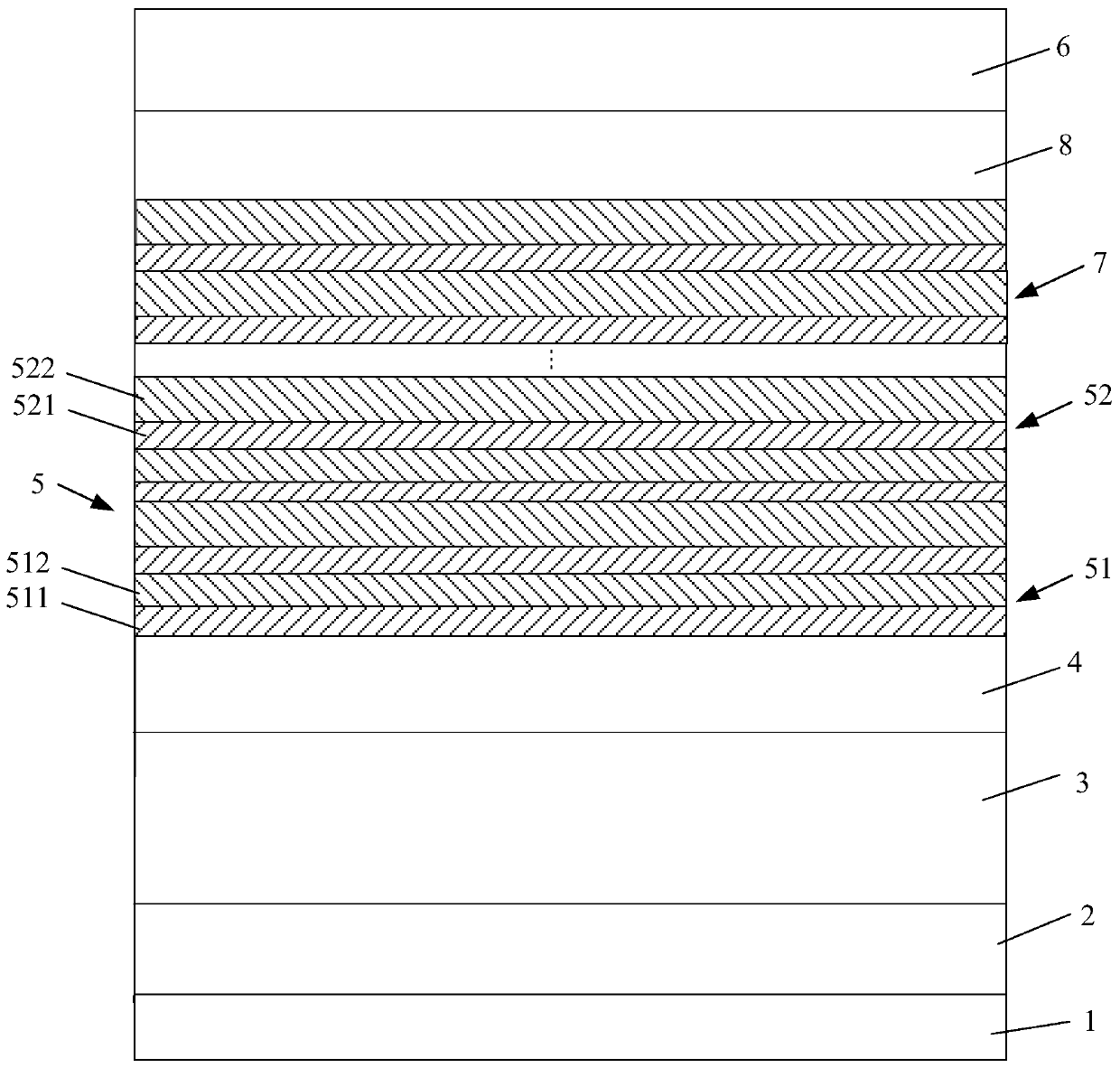
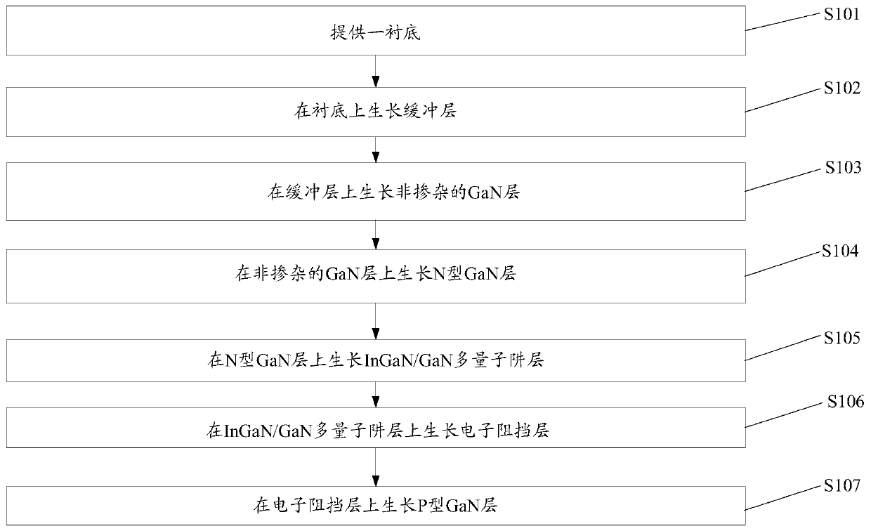
[0028] figure 1 is a schematic structural view of a light-emitting diode epitaxial wafer provided by an embodiment of the present disclosure, as shown in figure 1 As shown, the light-emitting diode epitaxial wafer includes a substrate 1 and a buffer layer 2 sequentially stacked on the substrate 1, an undoped GaN layer 3, an N-type GaN layer 4, an InGaN / GaN multi-quantum well layer 5, and a P-type GaN layer6.

[0029] The InGaN / GaN multi-quantum well layer 5 includes a plurality of alternately stacked first recombination units 51 and second recombination units 52. The first recombination unit 51 includes a first InGaN well layer 511 and a first GaN barrier layer 512 stacked in sequence. The second recombination unit 52 includes a ...


PUM

PropertyMeasurementUnit
thicknessaaaaaaaaaa
thicknessaaaaaaaaaa
thicknessaaaaaaaaaa

Abstract

The invention discloses a light-emitting diode epitaxial wafer and a preparation method thereof, and belongs to the technical field of light-emitting diodes. An InGaN / GaN multi-quantum well layer in the light-emitting diode epitaxial wafer is arranged to comprise a plurality of first composite units and a plurality of second composite units which are alternately stacked, wherein the first composite unit comprises a first InGaN well layer and a first GaN barrier layer which are stacked; the second composite unit comprises a second InGaN well layer and a second GaN barrier layer which are stacked; the thickness of the first InGaN well layer is less than that of the second InGaN well layer; the second InGaN well layer ensures the luminous efficiency of the InGaN / GaN multi-quantum well layer;and the first InGaN well layer with the thickness being less than that of the second InGaN well layer can reduce the In content in the second InGaN well layer while the luminous efficiency is ensured,and the polarization effect caused by the first InGaN well layer is reduced. The second GaN barrier layer with the thickness being greater than that of the first GaN barrier layer is arranged to playa role in blocking electrons, the number of electrons and holes compounded in the InGaN / GaN multi-quantum well layer is ensured, and the light-emitting effect of the InGaN / GaN multi-quantum well layer is integrally improved.

Description

technical field [0001] The disclosure relates to the technical field of light-emitting diodes, in particular to epitaxial wafers of light-emitting diodes and a preparation method thereof. Background technique [0002] Light-emitting diodes are semiconductor electronic components that can emit light. Light-emitting diodes are widely used in lighting equipment such as traffic lights, car interior and exterior lights, urban landscape lighting, and indoor and outdoor display screens. When preparing a light-emitting diode, it is necessary to prepare a light-emitting diode epitaxial wafer first, and then perform subsequent fabrication through the light-emitting diode epitaxial wafer to obtain a light-emitting diode. [0003] The structure of the epitaxial layer of the light-emitting diode mainly includes: the substrate and the buffer layer grown on the substrate in turn, the non-doped GaN layer, the N-type GaN layer, the InGaN / GaN multi-quantum well layer and the P-type GaN layer....

Claims


Application Information

Patent Timeline
Patent Type & Authority Applications(China)
IPC IPC(8): H01L33/00H01L33/06H01L33/14H01L33/32
CPCH01L33/0075H01L33/06H01L33/145H01L33/32
Inventor 姚振从颖董彬忠李鹏
Owner HC SEMITEK SUZHOU
Why Eureka
Try Eureka