Electronic chip packaging structure and method

A packaging method and technology for electronic chips, applied in circuits, electrical components, electrical solid devices, etc., can solve the problems of offsetting the efficiency of substrate assembling, low efficiency, and time-consuming injection molding, achieving good dimensional stability, cost reduction, low cost effect

Pending Publication Date: 2020-04-28
姜凤明 +1
View PDF0 Cites 0 Cited by
  • Summary
  • Abstract
  • Description
  • Claims
  • Application Information

AI Technical Summary

Problems solved by technology

But because of the molded encapsulation process, the entire bottom surface uses the substrate
[0012] 3. The injection molding packaging process of the electronic chip molding packaging process takes a long time
If the area of ​​electronic products or devices is large, the efficiency of substrate panel formation will be basically offset
[0013] 4. For the cutting of non-rectangular finished products, laser cutting and water jet cutting are currently required to complete the process, and the efficiency is very low
[0014] Among the above reasons, especially the cost of the substrate accounts for more than half of the entire production cost

Method used


Image

  • Electronic chip packaging structure and method
  • Electronic chip packaging structure and method
  • Electronic chip packaging structure and method

Examples


specific Embodiment 2

[0063] The implementation steps of specific embodiment 2 are as follows:

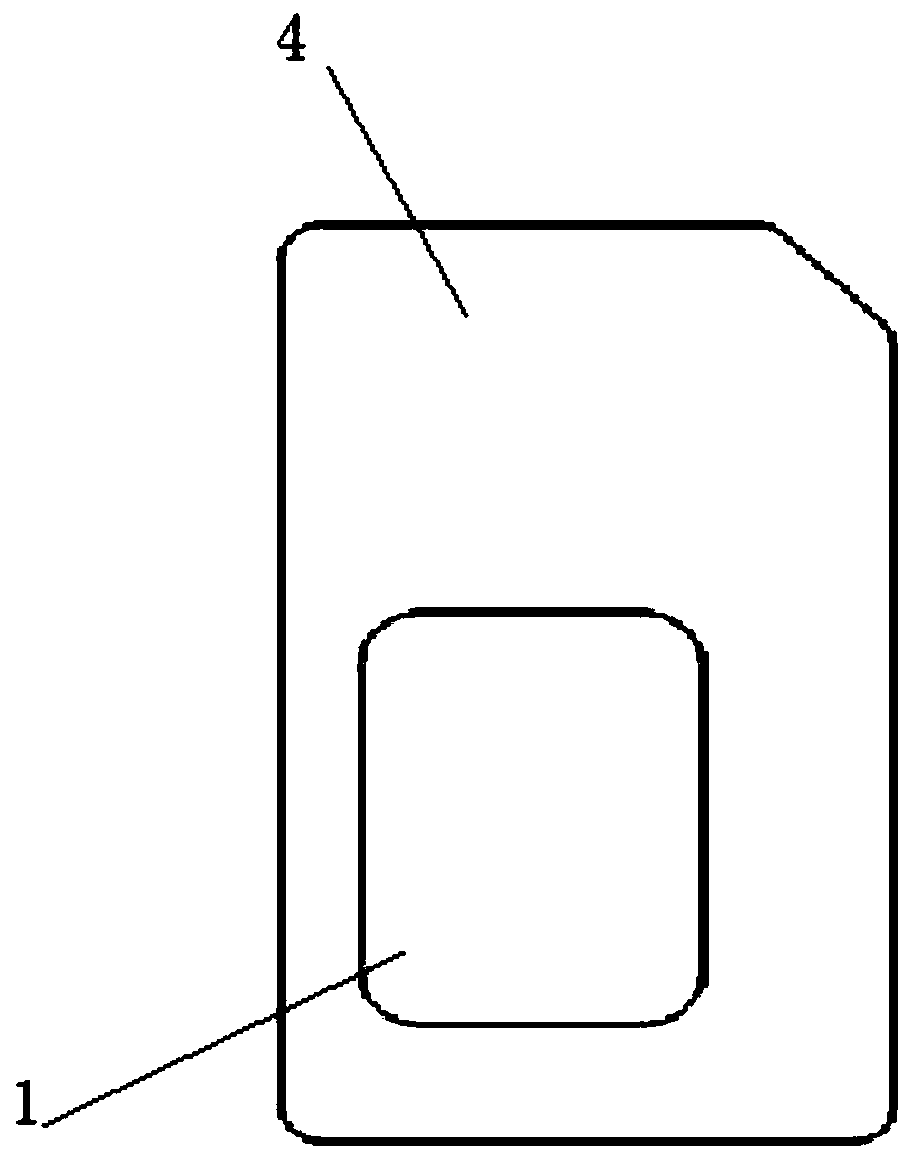
[0064] 1. Choose an aluminum alloy plate with a thickness of about 0.8mm, a low coefficient of thermal expansion, and high hardness --- aviation aluminum sheet as the finished product carrier 4.

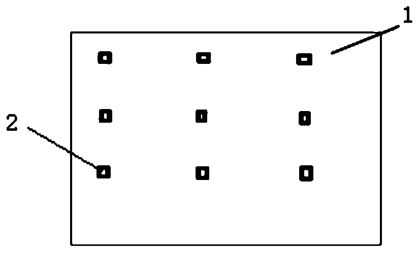
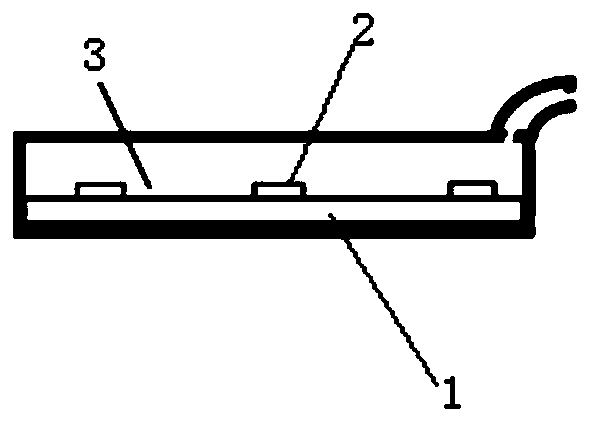
[0065] 2. CNC processing of aviation aluminum sheet. Mill groove 5 on one of the planes of the aviation aluminum sheet, and cut around the plane. Obtain the semi-finished product of the Internet of Things card carrier as shown in the figure, the size of the groove 5 and the substrate 1 have no clear size difference, which depends on the difference in thermal expansion coefficient between the various components and the tolerance formed in production. The groove 5 is a stepped groove. Since the chip 2 protrudes from the plane of the substrate 1, a stepped groove is provided to provide a mounting space for the chip 2 on the finished carrier 4. The first-level groove of the stepped groove is a rectangular struc...


PUM


Abstract

The invention provides an electronic chip packaging method in order to eliminate the cost disadvantage of the prior art. With the electronic chip packaging method adopted, the production cost of a whole process is effectively reduced. The electronic chip packaging method is characterized by comprising the following steps of: a, obtaining a finished product carrier, and forming a groove in the finished product carrier; b, mounting a chip on a substrate; and c, mounting the substrate with the chip into the groove.

Description

technical field [0001] The invention relates to the technical field of chip packaging, in particular to an electronic chip packaging structure and method thereof. Background technique [0002] At present, electronic chips are usually encapsulated by a molding packaging process. Molded packaging can ensure the mechanical strength, airtightness and electrical connection performance of the finished electronic device. One or more electronic chips are molded and packaged to form an electronic device. [0003] The continuous development of molding and packaging technology has produced many branches of technology. These include BGA packaging process and LGA packaging process. Both of these two packaging processes lead the pins of the chip through the substrate circuit to the bottom contact point of the electronic device formed after the molded package. The purpose of the BGA packaging process is to solder these contact points, so solder balls are added on the contact points; an...

Claims


Application Information

Patent Timeline
Patent Type & Authority Applications(China)
IPC IPC(8): H01L21/56H01L23/31H01L25/16
CPCH01L21/56H01L23/3107H01L25/165
Inventor 姜凤明王海泉
Owner 姜凤明
Why Eureka
Try Eureka