LED chip and preparation method thereof
A technology of LED chips and insulating layers, which is applied in the direction of electrical components, circuits, semiconductor devices, etc., can solve the problems of loss of luminous area, insulation problems of hole walls, and reduction of light efficiency, so as to achieve good application prospects, relieve current congestion, and improve the preparation process. simple effect
- Summary
- Abstract
- Description
- Claims
- Application Information
AI Technical Summary
Problems solved by technology
Method used
Image
Examples
Embodiment 1
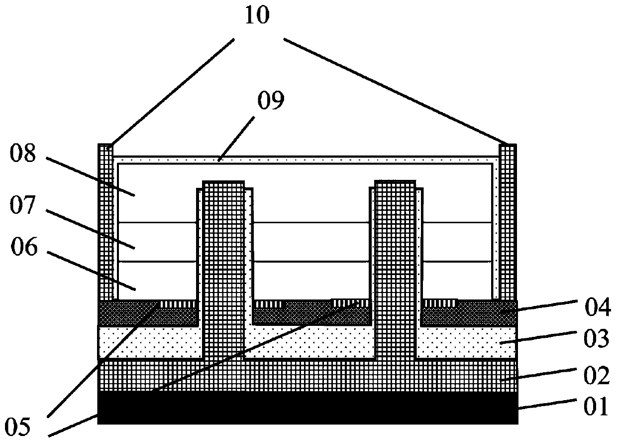
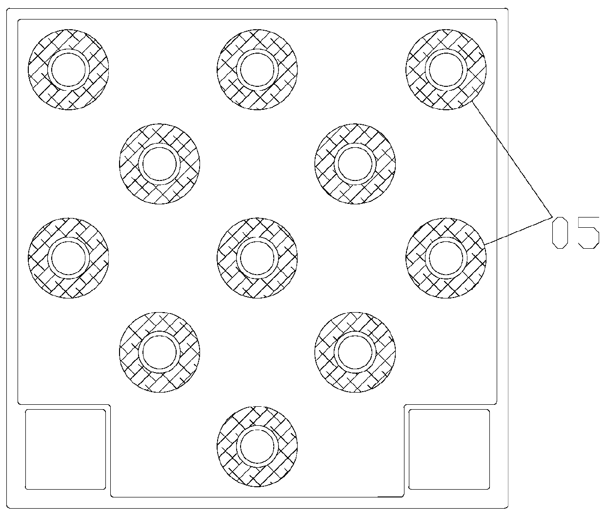
[0042] A kind of LED chip, refer to figure 1 As shown, it includes conductive substrate 01, n-electrode contact layer 02, first insulating layer 03, p-contact mirror metal and protective layer 04, ring-shaped CBL layer 05, and p-type GaN layer 06 arranged in order from bottom to top , InGaN / GaN multi-quantum well light-emitting layer 07, n-type GaN layer 08, second insulating layer 09, and P electrode 10; the embedded columnar N electrode layer 02 radially penetrates the first insulating layer 03, p-contact mirror in sequence The metal and protective layer 04, the annular CBL layer 05, the p-type GaN layer 06, and the InGaN / GaN multi-quantum well light-emitting layer 07 form a columnar embedded n-electrode layer, which is finally in contact with the n-type GaN layer 08; the embedded columnar N The electrode layer 02 is connected to the conductive substrate 01 to form electrical conduction; the upper surface of the columnar embedded n-electrode layer is connected to n-GaN08 to ...
Embodiment 2
[0060] This embodiment provides an LED chip (LED-2). The difference from the chip of Embodiment 1 is mainly reflected in the structure of the CBL layer. The CBL layer of this embodiment is not a substantial material structure, but a P-GaN surface Corresponding positions of the passivation area are subjected to selective dimension etch strokes.
[0061] Correspondingly, in the preparation method of this embodiment, the preparation process of the CBL layer is a photolithography plus ICP etching process and a CBL ring structure. ICP etch using H 2 / Ar, ratio 8:1, upper power 160W lower power 70W, etching time 2min.
[0062] Other structures and methods are completely consistent with Example 1.
PUM
| Property | Measurement | Unit |
|---|---|---|
| thickness | aaaaa | aaaaa |
| thickness | aaaaa | aaaaa |
| thickness | aaaaa | aaaaa |
Abstract
Description
Claims
Application Information


