
A kind of fingerprint recognition module and preparation method thereof

A fingerprint recognition module and fingerprint recognition technology, applied in character and pattern recognition, acquisition/organization of fingerprints/palmprints, semiconductor/solid-state device manufacturing, etc. Ensure precise alignment

Active Publication Date: 2021-11-02
绥化市鸿骏智能科技有限公司
View PDF4 Cites 0 Cited by
  • Summary
  • Abstract
  • Description
  • Claims
  • Application Information

AI Technical Summary

Problems solved by technology

During the use of the existing biometric identification module, the functional area of ​​the biometric identification chip is easily damaged under the action of pressing force due to the long-term pressing of the biometric identification module

Method used


Image

  • A kind of fingerprint recognition module and preparation method thereof
  • A kind of fingerprint recognition module and preparation method thereof
  • A kind of fingerprint recognition module and preparation method thereof

Examples


Embodiment Construction

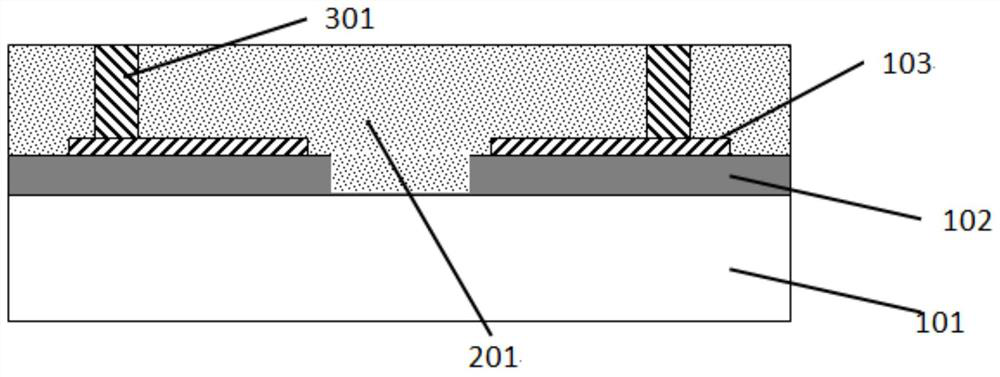
[0015] Such as Figure 1-Figure 9 Shown, a kind of preparation method of fingerprint identification module comprises the following steps:

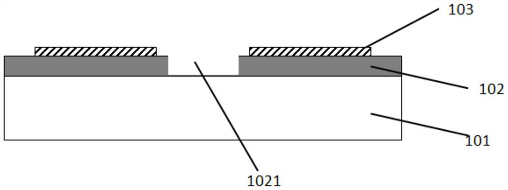
[0016] Such as figure 1 As shown, in step 1), a substrate 101 is provided, and the substrate has an opposite first surface and a second surface; in step 2), a first substrate is formed on the first surface of the substrate 101. a dielectric layer 102, forming a conductive wiring layer 103 on the first dielectric layer 102;

[0017] The material of the substrate 101 is glass, ceramics, plastic or silicon. The material of the first dielectric layer 102 is one or more of silicon nitride, silicon oxynitride, silicon oxide, silicon carbide, aluminum oxide, aluminum nitride, and the first dielectric layer 102 can be a single layer or multi-layer structure, the preparation method of the first dielectric layer 102 is PECVD method, ALD method or thermal oxidation method, and the material of the conductive wiring layer 103 is one of gold, silver,...


PUM

PropertyMeasurementUnit
thicknessaaaaaaaaaa
thicknessaaaaaaaaaa

Abstract

The invention relates to a method for preparing a fingerprint recognition module, the method comprising: providing a substrate having opposite first surfaces and second surfaces; forming a first dielectric layer and a conductive wiring layer on the first surface of the substrate; Form a slotted area in the first dielectric layer; form a conductive metal column on the conductive wiring layer; provide a carrier plate, set a release film and a fingerprint recognition chip on the carrier plate; A retaining wall structure is formed on the board, and an elastic buffer layer is bonded on the fingerprint identification functional area; solder balls are arranged in the area corresponding to the pad in the conductive wiring layer, and then the fingerprint identification chip is arranged on the on the conductive wiring layer, so that the elastic buffer layer is embedded into the slotted area, and the solder balls are melted and embedded into the corresponding retaining wall structure through a reflow soldering process; a plastic sealing layer is formed on the substrate , thinning the substrate from the second surface of the substrate.

Description

technical field [0001] The invention relates to the field of semiconductor packaging, in particular to a fingerprint recognition module and a preparation method thereof. Background technique [0002] In the existing biometric identification module, usually a hard encapsulation material layer is formed on the biometric identification chip, then the encapsulation material layer is thinned, and then a protective cover is provided on the thinned encapsulation material layer. During the use of the existing biometric identification module, since the biometric identification module is pressed many times for a long time, the functional area of ​​the biometric identification chip is easily damaged under the action of the pressing force. Contents of the invention [0003] The purpose of the present invention is to overcome the shortcomings of the above-mentioned prior art, and provide a fingerprint recognition module and a preparation method thereof. [0004] In order to achieve th...

Claims


Application Information

Patent Timeline
Patent Type & Authority Patents(China)
IPC IPC(8): H01L21/48H01L21/56H01L21/60H01L23/14H01L23/13H01L23/31H01L23/498G06K9/00
CPCH01L21/563H01L21/568H01L21/4853H01L24/81H01L23/14H01L23/13H01L23/3114H01L23/49816H01L23/49838H01L2224/81345G06V40/12H01L2224/81001H01L2224/11H01L2224/16225H01L2224/81H01L2924/181H01L2924/00012
Inventor 王桥
Owner 绥化市鸿骏智能科技有限公司
Learn More