Conductive material defect high-precision imaging detection method based on pulsed eddy current

A conductive material, pulsed eddy current technology, applied in the direction of material analysis, material analysis, material magnetic variables, etc. by electromagnetic means, can solve the problems of detection time influence, uncorrelated scanning speed and signal acquisition speed, low sensor accuracy, etc. Improved effectiveness and accuracy, rich data support, high defect scan detection resolution

Active Publication Date: 2020-05-08
LANZHOU INST OF PHYSICS CHINESE ACADEMY OF SPACE TECH
View PDF8 Cites 8 Cited by
  • Summary
  • Abstract
  • Description
  • Claims
  • Application Information

AI Technical Summary

Problems solved by technology

[0005](1) The sensor accuracy of the eddy current probe is low, and the sensor arrangement spacing is large, resulting in low resolution of the probe scanning defects, which may easily cause small defects to be missed
[0006](2) The scanning speed of the eddy current probe and the signal acquisition speed are irrelevant and do not match, resulting in the accuracy of defect information detection being easily affected by the hand speed of the inspector, directly affecting the defect Accuracy and effect of quantitative or imaging detection
Since the signal sampling rate is fixed during the inspection process, the inspection time is affected by the hand speed of the inspector, which makes the defect imaging inspection appear like Figure 1

Method used


Image

  • Conductive material defect high-precision imaging detection method based on pulsed eddy current
  • Conductive material defect high-precision imaging detection method based on pulsed eddy current
  • Conductive material defect high-precision imaging detection method based on pulsed eddy current

Examples


Embodiment Construction

[0026] The present invention will be described in detail below with reference to the accompanying drawings and examples.

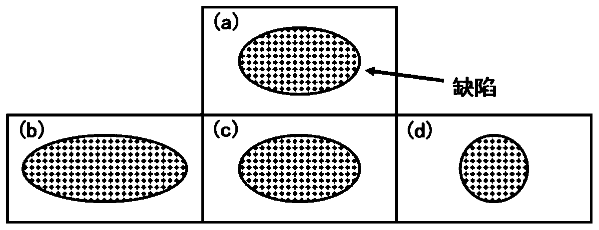
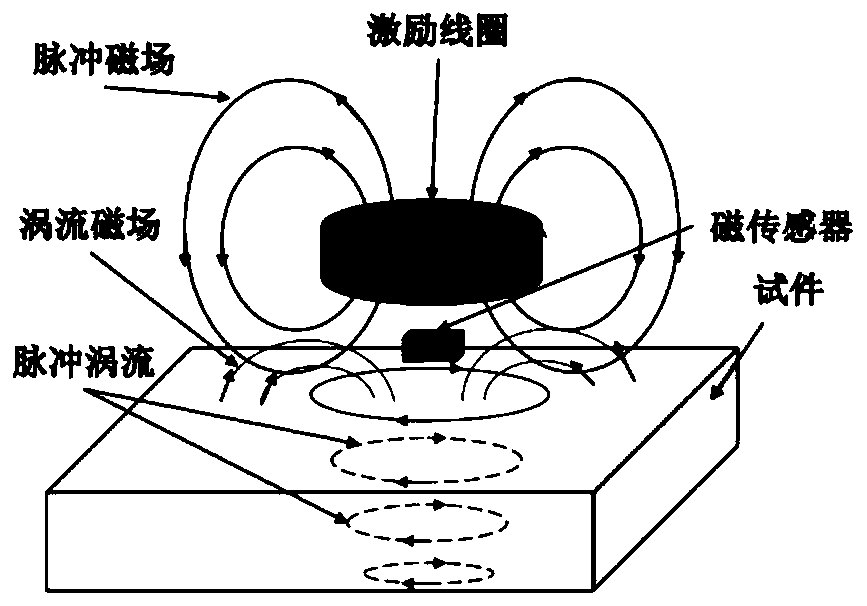
[0027] The invention provides a high-precision imaging detection method for conductive material defects based on pulsed eddy current. The principle of eddy current pulse nondestructive detection is as follows: figure 2 As shown, the pulsed magnetic field is induced by the excitation coil with pulsed voltage or current signal. When it is close to the surface of the conductor, the inside of the conductor forms a closed loop, and the electromagnetic induction effect occurs to generate a vortex-shaped induced current, that is, a pulsed eddy current. The eddy current will generate an eddy current magnetic field in space, and defects on the surface and inside of the conductor will affect the change of the eddy current magnetic field. Therefore, through the acquisition of the magnetic sensor, after signal processing and inversion, the surface and internal defects...


PUM


Abstract

The invention discloses a conductive material defect high-precision imaging detection method based on a pulsed eddy current. The method comprises the following steps: 1, arranging two rows of magneticsensors in an excitation magnetic field uniform region on the surface of a conductive material to be detected in an array manner, and arranging a second row of sensors in a gap position of the firstrow of sensors; 2, sending an acquisition instruction to the magnetic sensor array in the scanning detection process by utilizing a speed encoder provided with a distance measuring wheel; 3, processing an acquired magnetic sensor signal by using an equal spatial interpolation method to obtain a magnetic field characteristic image of the detected area; according to the invention, high-precision imaging detection of defects of the conductive material can be realized.

Description

technical field [0001] The invention belongs to the technical field of nondestructive testing, and in particular relates to a high-precision imaging detection method for conductive material defects based on pulsed eddy currents. Background technique [0002] A lot of equipment in the fields of aerospace, machinery manufacturing, nuclear power generation, petrochemical and military production are made of metal materials, such as aerospace equipment, armored vehicles, ships, pressure-bearing special equipment, etc., because these equipment often work at high temperatures Under the conditions of high pressure, high pressure, high speed and alternating heavy load, defects such as pits, cracks and corrosion will occur on the surface or inside of many key components. For example, during the flight of an aircraft, the fuselage will be subjected to various loads such as longitudinal stress, shear stress, and impact, and cracks and other defects are easily produced; engine blades are...

Claims


Application Information

Patent Timeline
Patent Type & Authority Applications(China)
IPC IPC(8): G01N27/90G01N27/904
CPCG01N27/9013G01N27/904G01N27/9006
Inventor 银鸿文轩杨生胜王鹢李存惠王俊庄建宏
Owner LANZHOU INST OF PHYSICS CHINESE ACADEMY OF SPACE TECH
Why Eureka
Try Eureka