Self-luminous display device and pixel internal and external compensation compatible circuit

A technology compatible with circuits and pixels, used in static indicators, instruments, etc., can solve the problems of large layout space, limited pixel density, long setting time, etc., to improve flexibility and compensation range, reduce the number, and drive signal simplicity. Effect

Inactive Publication Date: 2020-05-08
NANJING CEC PANDA LCD TECH
View PDF10 Cites 5 Cited by
  • Summary
  • Abstract
  • Description
  • Claims
  • Application Information

AI Technical Summary

Problems solved by technology

However, the current control mode has the following two problems: (1) the control current is weak current, which has high requirements for the design of the driver IC; (2) due to the influence of parasitic capacitance, the pixel compensation circuit of the current control mode requires a relatively long setting time to achieve compensation
In order to achieve better coupling and voltage retention effects, the size of the two capacitors needs to be designed to be sufficient. However, in a design with a higher pixel density, the capacitor will occupy a larger layout space, which limits the increase in pixel density.

Method used


Image

  • Self-luminous display device and pixel internal and external compensation compatible circuit
  • Self-luminous display device and pixel internal and external compensation compatible circuit
  • Self-luminous display device and pixel internal and external compensation compatible circuit

Examples


Embodiment Construction

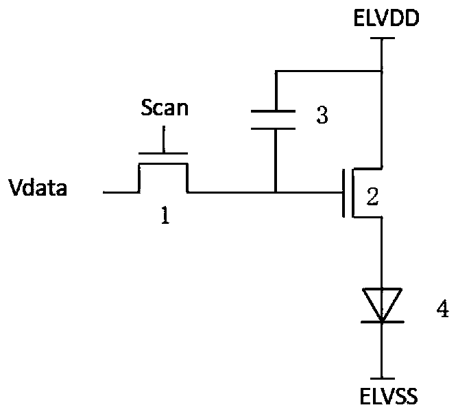
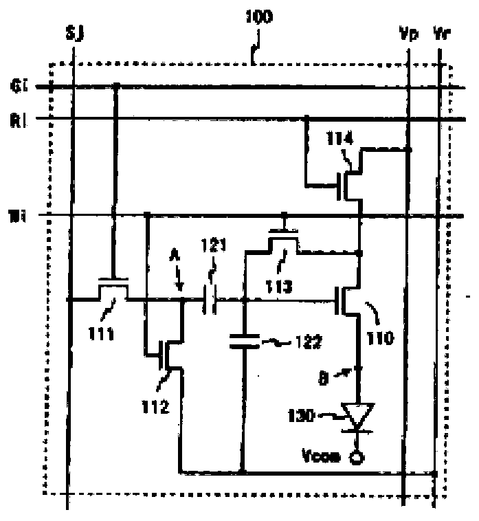
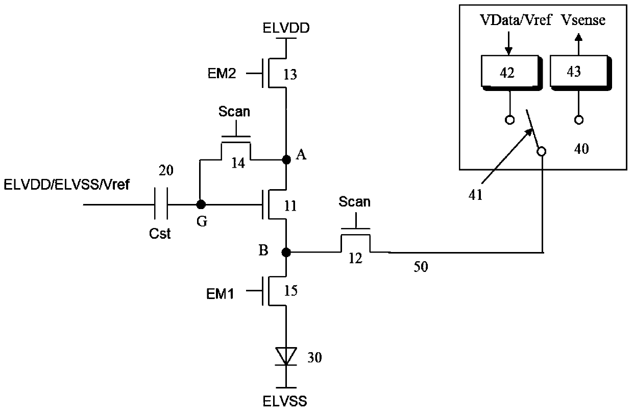
[0070] Below in conjunction with accompanying drawing and specific embodiment, further illustrate the present invention, should be understood that these embodiments are only for illustrating the present invention and are not intended to limit the scope of the present invention, after having read the present invention, those skilled in the art will understand various aspects of the present invention Modifications in equivalent forms all fall within the scope defined by the appended claims of this application.

[0071] In order to make the drawing concise, each drawing only schematically shows the parts related to the present invention, and they do not represent the actual structure of the product. In addition, to make the drawings concise and easy to understand, in some drawings, only one of the components having the same structure or function is schematically shown, or only one of them is marked. Herein, "a" not only means "only one", but also means "more than one".

[0072] ...


PUM


Abstract

The invention provides a pixel internal and external compensation compatible circuit. The pixel internal and external compensation compatible circuit is connected with a luminous element; the luminouselement is located between a first power supply and a second power supply, the compatible circuit is connected with a driving chip through a signal multiplexing line, and the driving chip is providedwith a switch, and a digital-to-analog converter and an analog-to-digital converter which can be connected with the switch; the compatible circuit further comprises a first driving TFT located between the first power supply and the luminous element, a first switching TFT located between the first driving TFT and the signal multiplexing line, a second switching TFT located between the first driving TFT and the first power supply, a storage capacitor located between the first driving TFT and the second power supply, a third switching TFT located between the first driving TFT and the storage capacitor and a fourth switching TFT located between the first driving TFT and the luminous unit. The compatible circuit has the capabilities of internal compensation and external compensation, and the flexibility and compensation range of pixel compensation are improved.

Description

technical field [0001] The present invention relates to the technical field of display panels, in particular to a self-luminous display device and a pixel internal and external compensation compatible circuit. Background technique [0002] In recent years, display devices have been developing in the direction of thinner, lighter and more flexible. Self-luminous displays include organic electroluminescent OLEDs, quantum dot electroluminescent QLEDs, and micro-electroluminescent Micro-LEDs. Self-luminous displays are in the These aspects have natural advantages. [0003] For the light-emitting element with self-luminous display, its luminous brightness has a positive correlation with the applied voltage and current. The relationship between luminous brightness and voltage will be affected by factors such as ambient temperature and usage time. Therefore, it is difficult to control the brightness uniformity and stability of the self-luminous display by adopting the method of v...

Claims


Application Information

Patent Timeline
Patent Type & Authority Applications(China)
IPC IPC(8): G09G3/32G09G3/3233
CPCG09G3/32G09G3/3233
Inventor 黄洪涛
Owner NANJING CEC PANDA LCD TECH
Why Eureka
Try Eureka