Junction field effect transistor and electrostatic discharge structure thereof

A field effect tube and electrostatic discharge technology, applied in the direction of circuits, transistors, electrical components, etc., can solve problems such as large resistance, device damage, and increased voltage in the gate area 103, so as to avoid thermal breakdown and improve antistatic effect of ability

Active Publication Date: 2020-05-19
JOULWATT TECH INC LTD
View PDF7 Cites 0 Cited by
  • Summary
  • Abstract
  • Description
  • Claims
  • Application Information

AI Technical Summary

Problems solved by technology

As shown in the figure, between the drain D and the gate G, the P-type potential well of the N channel and the gate region 103 can be regarded as a PN junction 106 opposite to the forward ESD current, when the ESD current When it comes, the PN junction 106 is broken down by the avalanche, and at this time the ESD current is poured into the gate region 103, and the bulk resistance 107 in the gate region 103 usually has a large resistance value, causing the voltage of the gate region 103 to increase rapidly and heat, thus causing damage to the device

Method used


Image

  • Junction field effect transistor and electrostatic discharge structure thereof
  • Junction field effect transistor and electrostatic discharge structure thereof
  • Junction field effect transistor and electrostatic discharge structure thereof

Examples


Embodiment Construction

[0031] The present invention will be described in detail below in conjunction with the specific embodiments shown in the accompanying drawings, but these embodiments do not limit the present invention, those of ordinary skill in the art make structural, method, or functional changes based on these embodiments All are included in the scope of protection of the present invention.

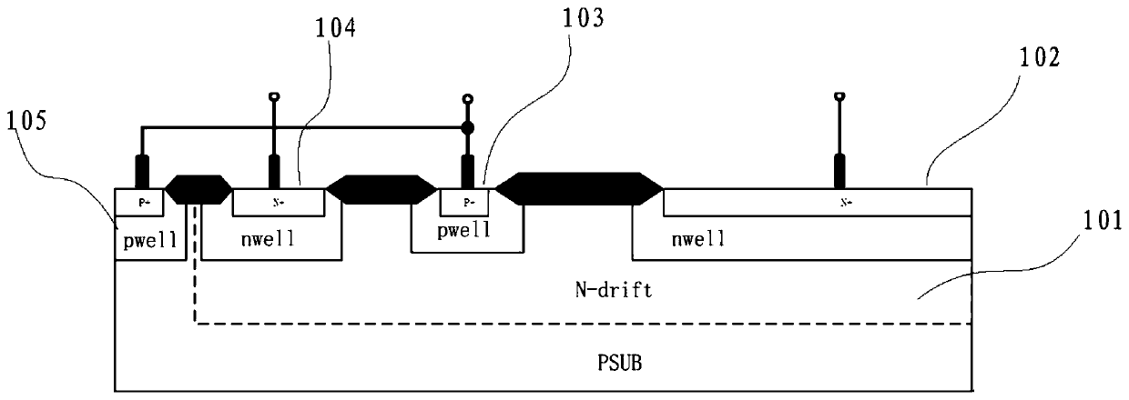
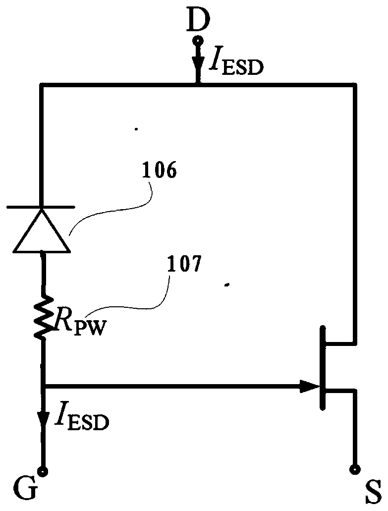
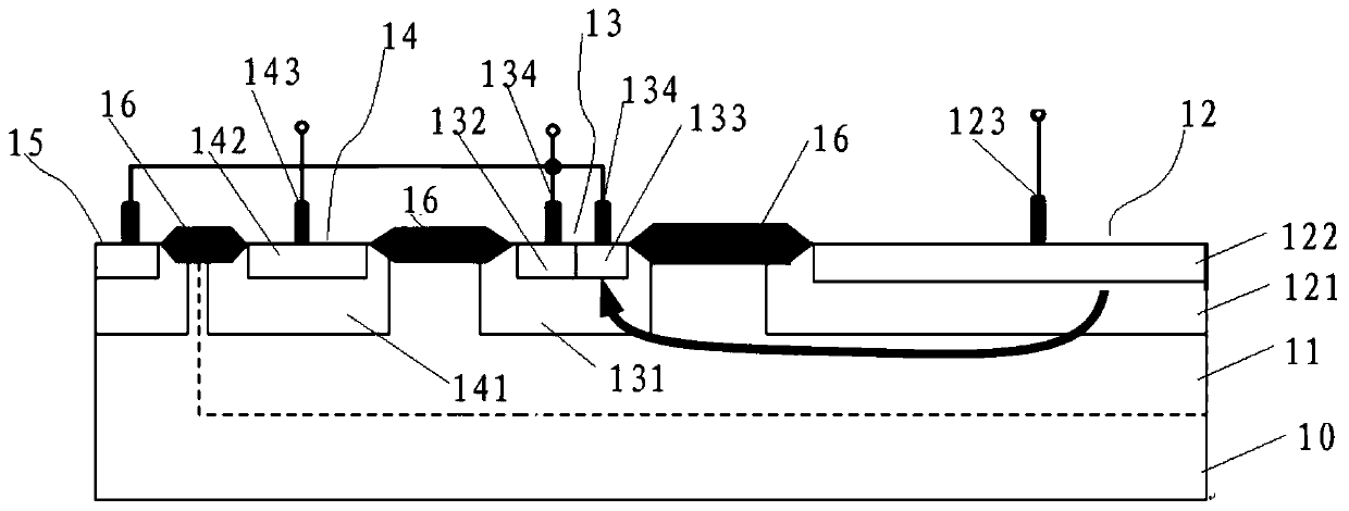
[0032] The invention is a junction field effect transistor with an electrostatic discharge structure. By inserting a heavily doped region with a different conductivity type from the gate region in the gate region, a parasitic triode path is formed with the drain end. When static electricity occurs, the drift The PN junction between the region and the gate potential well forms an avalanche breakdown. When the voltage drop on the gate potential well reaches 0.7V, the parasitic triode will be turned on, and then the electrostatic current will be discharged through the parasitic triode due to the NPN triod...


PUM


Abstract

The invention provides a junction field effect transistor and an electrostatic discharge structure thereof. The junction field effect transistor comprises a source region and a drain region, and a first gate region disposed between the source region and the drain region, wherein the first gate region comprises a first potential well and a first heavily doped region of a first conductivity type, asecond heavily doped region of a second conductivity type and a gate electrode, wherein the first heavily doped region and the second heavily doped region are arranged in the first potential well in parallel and are in ohmic contact with the gate electrode arranged on the surface of the first gate region. When static electricity occurs, avalanche breakdown is formed by a PN junction between a drift region and a grid potential well, a parasitic triode structure is triggered, and then, static current is discharged through the parasitic triode, so that the antistatic capacity of the device is improved.

Description

technical field [0001] The invention relates to the technical field of semiconductors, in particular to a junction field effect transistor and an electrostatic discharge structure thereof. Background technique [0002] Electrostatic discharge (ESD: Electrostatic Discharge) should be the main culprit that causes all electronic components or integrated circuit systems to cause excessive electrical stress (EOS: Electrical Over Stress) damage. Because static electricity usually has a very high instantaneous voltage (> several thousand volts), this damage is devastating and permanent, and it will cause the circuit to burn directly. According to the statistics of the National-Semiconductor Corporation (National-Semiconductor), 38% of today's integrated circuit failure products are caused by ESD / EOS. [0003] The PN junction is the basic unit in existing semiconductor devices. In the ESD protection of semiconductor devices, it is necessary to consider how to prevent the PN junc...

Claims


Application Information

Patent Timeline
IPC IPC(8): H01L29/423H01L29/45H01L29/808H01L27/02
CPCH01L29/4232H01L29/45H01L29/808H01L27/0259
Inventor 胡涛陆阳
Owner JOULWATT TECH INC LTD
Why Eureka
Try Eureka