Semiconductor structure capable of reducing switching loss and manufacturing method

A switching loss and semiconductor technology, which is applied in semiconductor/solid-state device manufacturing, semiconductor devices, electrical components, etc., can solve the problems of excessive gate charge and large device switching loss, and achieve the effect of reducing switching loss and reducing manufacturing costs

Pending Publication Date: 2020-05-19
WUXI NCE POWER
View PDF0 Cites 9 Cited by
  • Summary
  • Abstract
  • Description
  • Claims
  • Application Information

AI Technical Summary

Problems solved by technology

[0005] The purpose of the invention is to overcome the problems of excessive gate charge and excessive device switching loss in the prior art, and provide a semi

Method used


Image

  • Semiconductor structure capable of reducing switching loss and manufacturing method
  • Semiconductor structure capable of reducing switching loss and manufacturing method
  • Semiconductor structure capable of reducing switching loss and manufacturing method

Examples


Embodiment 1

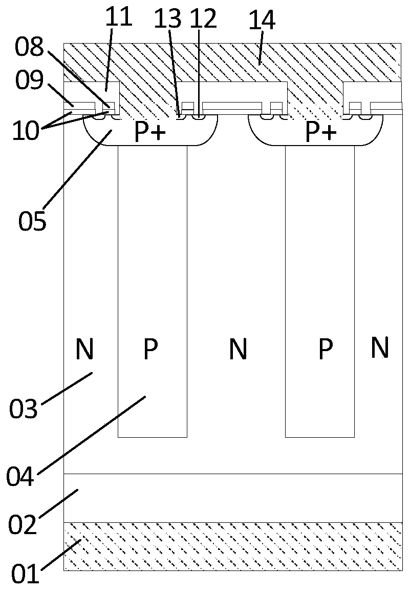
[0063] refer to figure 1 , is a semiconductor structure for reducing switching loss, taking an N-type planar super-junction power semiconductor device as an example, including a drain 01, an N-type substrate 02, and an N-type epitaxial layer 03 that are sequentially stacked from bottom to top; The material of the drain 01 is preferably metal, and the material of the N-type substrate 02 may be silicon.

[0064] A plurality of P-type columns 04 are arranged in the N-type epitaxial layer 03, and the plurality of P-type columns 04 are distributed at intervals, and each of the P-type columns 04 faces from the upper surface of the N-type epitaxial layer 03 to Extend down.

[0065] The upper end of the P-type column 04 forms a P-type body region 05, and the P-type body region 05 is heavily doped to form an N-type first source region 13, and the P-type body regions on both sides of the N-type first source region 13 The N-type second source region 12 is formed by heavy doping in the...

Embodiment 2

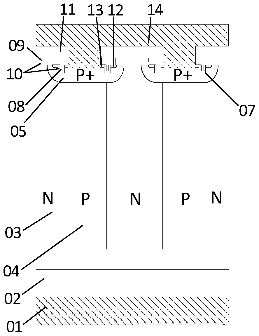
[0072] refer to figure 1 , is a semiconductor structure for reducing switching loss, taking an N-type planar super-junction power semiconductor device as an example, including a drain 01, an N-type substrate 02, and an N-type epitaxial layer 03 that are sequentially stacked from bottom to top; The material of the drain 01 is preferably metal, and the material of the N-type substrate 02 may be silicon.

[0073] A plurality of P-type columns 04 are arranged in the N-type epitaxial layer 03, and the plurality of P-type columns 04 are distributed at intervals, and each of the P-type columns 04 faces from the upper surface of the N-type epitaxial layer 03 to Extend down.

[0074] The upper end of the P-type column 04 forms a P-type body region 05, and the P-type body region 05 is heavily doped to form an N-type first source region 13, and the P-type body regions on both sides of the N-type first source region 13 The N-type second source region 12 is formed by heavy doping in the...

Embodiment 3

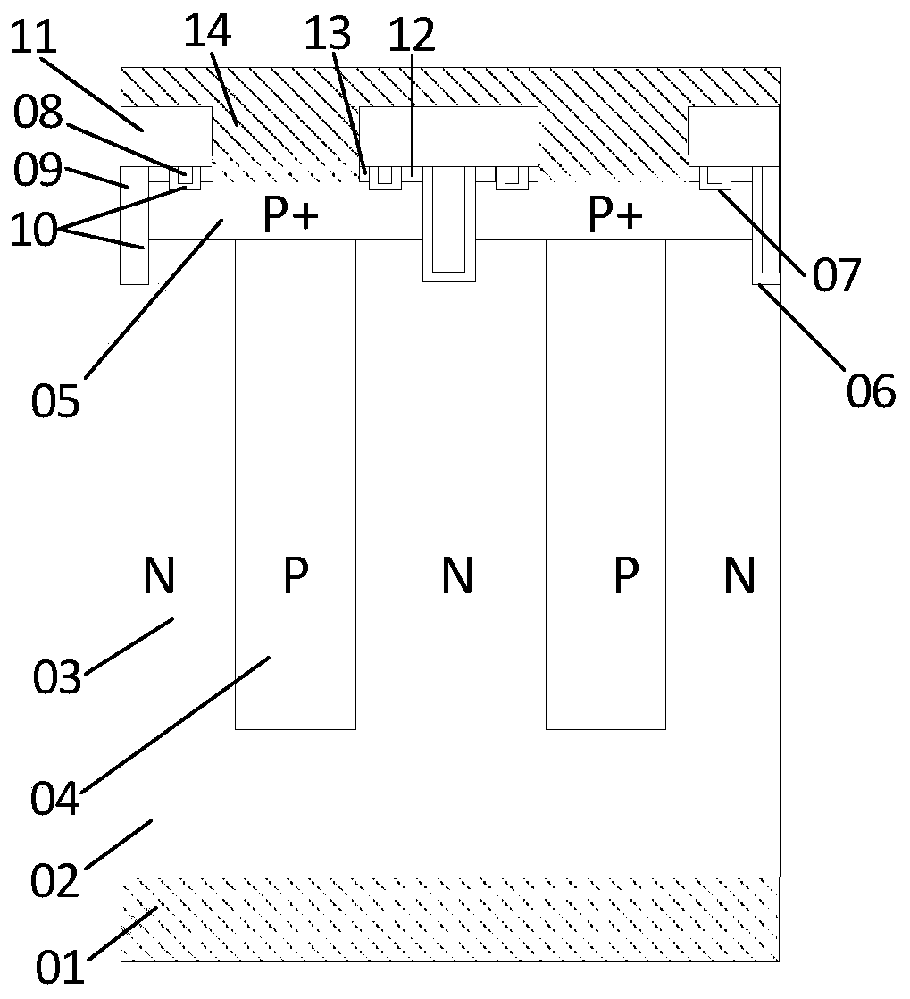
[0081] refer to image 3 , is a semiconductor structure for reducing switching loss, taking an N-type planar super-junction power semiconductor device as an example, including a drain 01, an N-type substrate 02, and an N-type epitaxial layer 03 that are sequentially stacked from bottom to top; The material of the drain 01 is preferably metal, and the material of the N-type substrate 02 may be silicon.

[0082] A plurality of P-type columns 04 are arranged in the N-type epitaxial layer 03, and the plurality of P-type columns 04 are distributed at intervals, and each of the P-type columns 04 faces from the upper surface of the N-type epitaxial layer 03 to Extend down.

[0083] The upper end of the P-type column 04 forms a P-type body region 05, and the P-type body region 05 is heavily doped to form an N-type first source region 13, and the P-type body regions on both sides of the N-type first source region 13 The N-type second source region 12 is formed by heavy doping in the bo...


PUM


Abstract

The invention relates to a semiconductor structure capable of reducing a switching loss and a manufacturing method. A drain electrode, a first conductive type substrate and a first conductive type epitaxial layer are sequentially arranged in a stacked mode from bottom to top; a plurality of second conductive type body regions are formed in the first conductive type epitaxial layer, the plurality of second conductive type body regions are distributed at intervals; heavily doping is performed in the second conductive type body regions to form a first conductive type second source region, and heavily doping is performed in the second conductive type body regions on one side of the first conductive type second source region to form a first conductive type first source region; a control gate structure is arranged between the first conductive type first source region and the first conductive type second source region which are adjacent to each other; a virtual gate structure is arranged on one side, far away from the first conductive type first source region, of the first conductive type second source region; an insulating dielectric layer is deposited on an upper surface of the semiconductor structure for reducing the switching loss; and at a middle position of the first conductive type first source region, a connecting hole is formed downwards from the upper surface of the insulating dielectric layer, and the connecting hole extends downwards into the first conductive type first source region.

Description

technical field [0001] The invention relates to a semiconductor device and a manufacturing method thereof, in particular to a semiconductor structure and a manufacturing method for reducing switching loss. Background technique [0002] As we all know, in the application of MOS device products, the power loss of the device itself is composed of conduction loss and switching loss. In the high-voltage and high-frequency working environment, the power loss is mainly switching loss, and the switching loss is mainly determined by the parasitic capacitance of the device. . [0003] In conventional design, in order to reduce the switching loss of the device in a high-voltage and high-frequency working environment, that is, to reduce the parasitic capacitance of the device, the characteristic on-resistance Rsp of the device will increase, that is, the conduction loss will increase; [0004] Such as Figure 12 As shown, taking the existing N-type super-junction planar gate MOS device...

Claims


Application Information

Patent Timeline
IPC IPC(8): H01L29/78H01L29/06H01L21/336
CPCH01L29/0634H01L29/66712H01L29/66734H01L29/7802H01L29/7813
Inventor 朱袁正杨卓周锦程
Owner WUXI NCE POWER
Why Eureka
Try Eureka