Electron multiplier device and manufacturing method thereof

An electron multiplier and a manufacturing method technology, which are applied in the fields of electronic technology and mass spectrometry analysis, can solve the problems of increasing the rejection rate of the channel electron multiplier, high temperature requirements, and increasing the manufacturing cost, so as to make up for difficult processing technology, save costs, simple structure

Inactive Publication Date: 2020-05-22
SHANGHAI YUDA IND
View PDF5 Cites 0 Cited by
  • Summary
  • Abstract
  • Description
  • Claims
  • Application Information

AI Technical Summary

Problems solved by technology

In this process, the requirements for processing machines and processing accuracy are relatively high, which greatly increases the production cost.
[0

Method used


Image

  • Electron multiplier device and manufacturing method thereof
  • Electron multiplier device and manufacturing method thereof

Examples


Embodiment Construction

[0030] The present invention will be described in detail below in conjunction with specific embodiments. The following examples will help those skilled in the art to further understand the present invention, but do not limit the present invention in any form. It should be noted that those skilled in the art can make several changes and improvements without departing from the concept of the present invention. These all belong to the protection scope of the present invention.

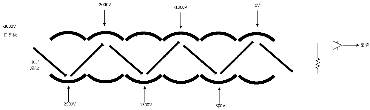
[0031] Such as Figure 1 to Figure 2 As shown, an electron multiplier device provided according to the present invention includes: electrodes 1; six pairs of electrodes 1; two pairs of electrodes 1 arranged in parallel; and electrodes 1 in the shape of convex lenses. The electrode 1 is made of a glass insulator; the electrode 1 is made of a ceramic sheet insulator; the glass insulator is coated with a metal layer; the ceramic sheet insulator is coated with a metal layer; the thickness of the metal layer...


PUM

PropertyMeasurementUnit
Thicknessaaaaaaaaaa

Abstract

The present invention provides an electron multiplier device. The device comprises: six pairs of electrodes (1); every two electrodes (1) are arranged in parallel; the electrodes (1) are all convex lens-shaped; the electrodes (1) are formed by glass insulators; and the electrodes (1) are formed by ceramic chip insulators. The electron multiplier device is simple in structure, only the six pairs ofparallel electrodes are arranged, the cost is saved while the performance is guaranteed, and the profit margin of a product can be effectively improved; and the defect that the existing product processing technology is difficult is overcome, and the method is of great significance to the iteration of the technology.

Description

technical field [0001] The present invention relates to the fields of electronic technology and mass spectrometry, in particular to an electron multiplier device and a manufacturing method thereof, especially a manufacturing method and structure of a high-performance electron multiplier. Background technique [0002] The channel electron multiplier (channeltron electron multiplier, CEM) is a vacuum device based on the principle of secondary electron emission as a weak signal amplification and detection. It not only has the advantages of simple structure, large gain, low power consumption, small size and simple power supply method. More importantly, it is also a highly sensitive and multifunctional detection device. It can directly detect electrons, ions, vacuum ultraviolet photons, neutral particles and α, β, γ rays, etc. without any conversion and high efficiency. At present, it is widely used at home and abroad. In addition to being used as an independent detector in mas...

Claims


Application Information

Patent Timeline
IPC IPC(8): H01J43/24H01J9/12
CPCH01J43/24H01J9/125
Inventor 胡波于佳佳景加荣孙露露唐朝阳胡继闯周旭沈辉罗勇
Owner SHANGHAI YUDA IND
Why Eureka
Try Eureka