Dual-node-upset-resistant D latch applied to high-frequency circuit

A technology of double-node flipping and high-frequency circuits, which is applied in the direction of improving reliability and improving the reliability of field effect transistors, etc., and can solve problems such as multiple hardware, large power consumption and area, and affecting hardening performance.

Pending Publication Date: 2020-05-26
ZHONGBEI UNIV
View PDF0 Cites 0 Cited by
  • Summary
  • Abstract
  • Description
  • Claims
  • Application Information

AI Technical Summary

Problems solved by technology

[0003] The purpose of the present invention is to solve the problem that the traditional anti-charge sharing D-latch consumes more hardware, consumes more power consumption and area, a

Method used


Image

  • Dual-node-upset-resistant D latch applied to high-frequency circuit
  • Dual-node-upset-resistant D latch applied to high-frequency circuit

Examples


Embodiment Construction

[0058] The following will clearly and completely describe the technical solutions in the embodiments of the present invention with reference to the accompanying drawings in the embodiments of the present invention. Obviously, the described embodiments are only some, not all, embodiments of the present invention. Based on the embodiments of the present invention, all other embodiments obtained by persons of ordinary skill in the art without making creative efforts belong to the protection scope of the present invention.

[0059] It should be noted that, in the case of no conflict, the embodiments of the present invention and the features in the embodiments can be combined with each other.

[0060] The present invention will be further described below in conjunction with the accompanying drawings and specific embodiments, but not as a limitation of the present invention.

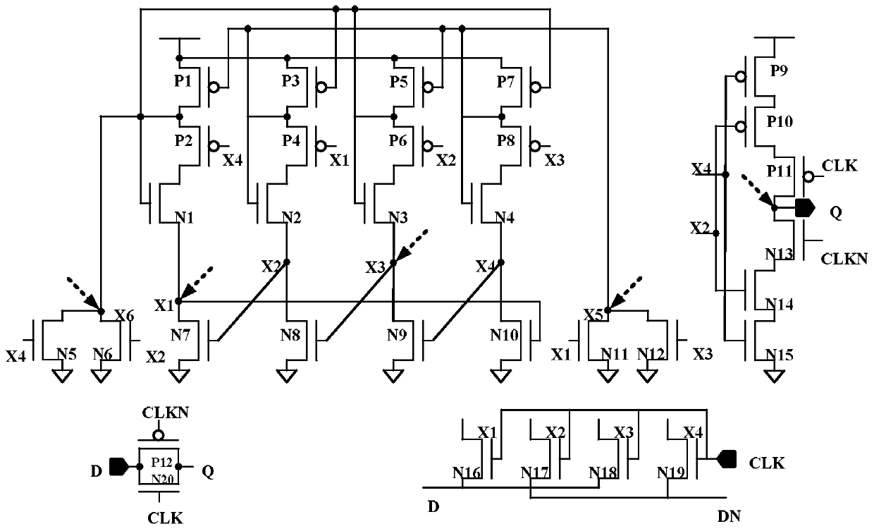
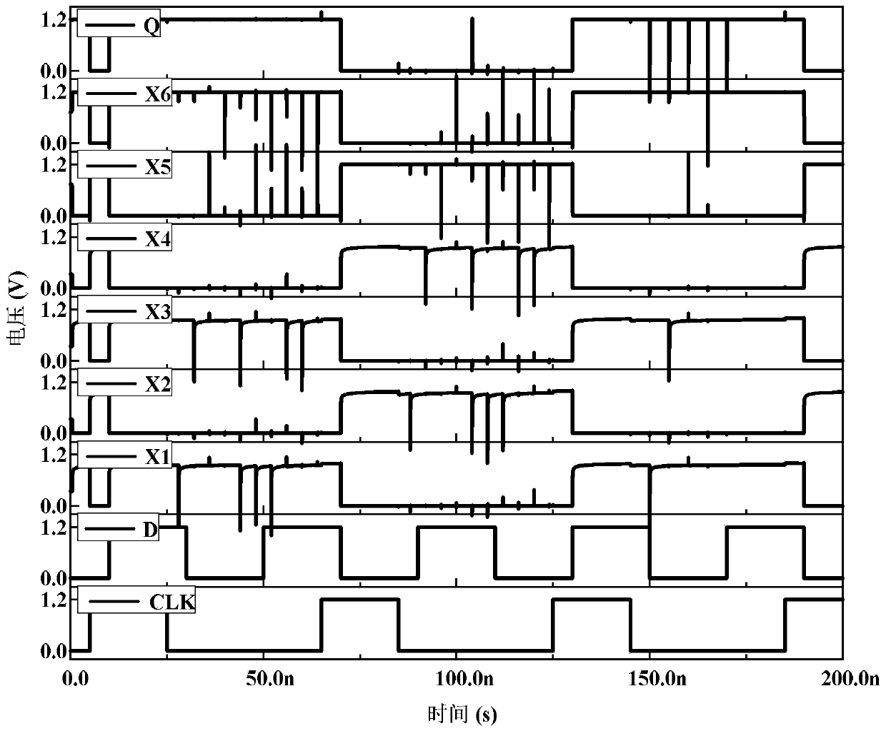
[0061] see figure 1 Describe this embodiment mode. The anti-double-node flipping D-latch described in this...


PUM


Abstract

The invention discloses a dual-node-upset-resistant D latch applied to a high-frequency circuit, which belongs to the field of anti-core reinforcement in reliability of integrated circuits. The problems that a traditional D latch resistant to charge sharing needs to consume more hardware and is large in power consumption and area, and the reinforcement performance is seriously affected due to moresensitive nodes are solved. The D latch comprises 20 NMOS transistors N1 to N20 and 12 PMOS transistors P1 to P12, and only 32 transistors are needed to construct the D latch, so that the area andthe power consumption overhead of the D latch are reduced. An input signal D can be directly transmitted to the output end of an output signal D through the transmission gates constructed by the transistors N20 and P12, so that the transmission delay is reduced. The D latch provided by the invention is suitable for being applied to high-frequency circuits, and is particularly suitable for aerospace, aerospace flight, nuclear power stations and the like with nuclear radiation effects.

Description

technical field [0001] The invention belongs to the field of anti-nuclear hardening in integrated circuit reliability. Background technique [0002] D latches are widely used in various digital integrated circuits, such as decoders and timing control circuits. However, since the latch has the function of storing information, radiation particles will change the information it holds, thus causing errors in the electronic system. With the advancement of integrated circuit technology, due to the influence of charge sharing, the flipping phenomenon has changed from the previous flipping of one node to the flipping of two nodes. However, the existing anti-charge sharing D latch requires more than 70 transistors, which requires more hardware, has a larger area and power consumption, and has more than 10 sensitive nodes. The more sensitive nodes, the more nodes are blocked. The higher the attack probability, the worse the reliability of the system, which seriously affects the hard...

Claims


Application Information

Patent Timeline
IPC IPC(8): H03K19/003
CPCH03K19/00315
Inventor 郭靖杜芳芳
Owner ZHONGBEI UNIV
Why Eureka
Try Eureka