Thin film packaging structure, thin film packaging method and concave hole design method

A technology of thin film packaging and concave holes, which is applied in the manufacture of electrical components, electrical solid devices, semiconductor/solid devices, etc., can solve the problems of increased waiting time, poor production efficiency, increased process time, etc., to reduce the contact angle and improve Flattening effect, wettability improvement effect

Inactive Publication Date: 2020-05-29
INCOFLEX SEMICON TECH CO LTD
View PDF18 Cites 0 Cited by
  • Summary
  • Abstract
  • Description
  • Claims
  • Application Information

AI Technical Summary

Problems solved by technology

However, increasing the thickness of the organic ink will affect the bending radius of the flexible panel, and increase material consumption and process time; and the current practice of increasing the waiting time for planarization will also increase the process time, resulting in poor production efficiency

Method used


Image

  • Thin film packaging structure, thin film packaging method and concave hole design method
  • Thin film packaging structure, thin film packaging method and concave hole design method
  • Thin film packaging structure, thin film packaging method and concave hole design method

Examples


Embodiment Construction

[0022] The terms "first", "second", etc. used herein do not specifically refer to a sequence or order, nor are they used to limit the present application, but are only used to distinguish components or operations described with the same technical terms. .

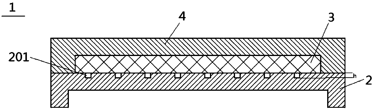
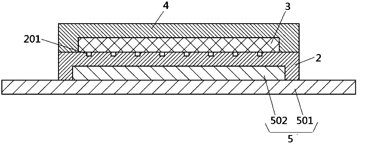
[0023] An embodiment of the present invention discloses a thin film encapsulation structure 1, please refer to Figure 1-4 As shown, it is applied to the thin film encapsulation of an organic light emitting diode (OLED) device 5, and the thin film encapsulation structure 1 includes a first inorganic encapsulation layer 2, an organic encapsulation layer 3 and a second inorganic encapsulation layer 4, wherein:

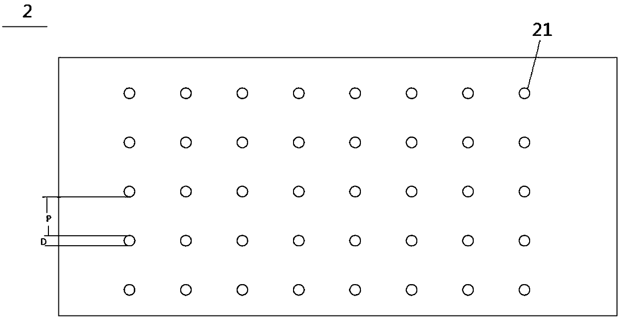
[0024] Please refer to figure 1 As shown, the first inorganic encapsulation layer 2 is arranged at the lower end of the thin film encapsulation structure 1. In the present invention, there is no special requirement for the material selection of the first inorganic encapsulation layer 2, and it can be selected by refe...


PUM


Abstract

The invention relates to a thin film packaging structure, a thin film packaging method and a concave hole design method. The thin film packaging structure comprises a first inorganic packaging layer,an organic packaging layer, and a second inorganic packaging layer; the first inorganic packaging layer is disposed at the lower end of the thin film packaging structure; the upper surface of the first inorganic packaging layer is provided with a plurality of concave holes; the organic packaging layer is arranged on the first inorganic packaging layer; the organic packaging layer is made of organic ink; and the organic packaging layer is formed by coating the organic ink on the first inorganic packaging layer, making the organic ink stand still and flattening the organic ink; and the second inorganic encapsulation layer is disposed on the organic encapsulation layer. According to the thin film packaging structure of the invention, the first inorganic packaging layer is formed, the plurality of concave holes are formed in the first inorganic packaging layer; the plurality of concave holes are designed; the contact angle between the organic ink and the first inorganic packaging layer isreduced by changing the hole diameter of each concave hole and the hole distance between two adjacent concave holes, and therefore, the wettability of the organic ink is improved, and the planarization effect of the organic ink is improved.

Description

technical field [0001] The invention relates to the technical field of thin-film packaging, in particular to a thin-film packaging structure, a thin-film packaging method, and a design method for concave holes on an inorganic packaging layer applied to thin-film packaging. Background technique [0002] At present, the thin-film packaging of Organic Light-Emitting Diode (OLED) devices is usually packaged in the stacking manner of inorganic layer / organic layer / inorganic layer, and the film formation method of the organic layer is to apply organic ink to the organic layer by inkjet printing. After laying on the inorganic layer, it is left to stand, and the organic ink is flattened and formed on the inorganic layer. [0003] In the prior art, when designing thin-film packaging, the contact surface between the inorganic layer and the organic layer is usually designed as a smooth plane, that is, the design is based on the intrinsic contact angle. However, in actual production, the...

Claims


Application Information

Patent Timeline
Patent Type & Authority Applications(China)
IPC IPC(8): H01L51/52
CPCH10K50/844
Inventor 陈秉宏
Owner INCOFLEX SEMICON TECH CO LTD
Why Eureka
Try Eureka