Inverted structure OLED device based on strong electron injection layer and manufacturing method thereof

An inverted structure and injection layer technology, which is applied in the direction of electrical solid-state devices, semiconductor/solid-state device manufacturing, electrical components, etc., can solve problems such as high energy consumption, high cost, and narrow manufacturing requirements, so as to improve work durability and improve The effect of electro-optical performance and excellent electronic performance

Inactive Publication Date: 2020-05-29
GUILIN UNIV OF ELECTRONIC TECH +2
View PDF0 Cites 1 Cited by
  • Summary
  • Abstract
  • Description
  • Claims
  • Application Information

AI Technical Summary

Problems solved by technology

[0002] In order to be compatible with the manufacturing process of OLED devices, the existing strong electron injection layers are mostly made from active alkali metals Ca, Ba, Cs, Li, Al, organic molecules pentacene and Liq, inorganic compounds LiF, CsF, Li 2 CO 3 and MoS 2 Thermal evaporation in the middle, more energy consumption, higher cost, narrower range of manufacturing needs that can be met

Method used


Image

  • Inverted structure OLED device based on strong electron injection layer and manufacturing method thereof
  • Inverted structure OLED device based on strong electron injection layer and manufacturing method thereof
  • Inverted structure OLED device based on strong electron injection layer and manufacturing method thereof

Examples


preparation example Construction

[0030] A preparation method for preparing the above-mentioned inverted structure OLED device, comprising the following steps:

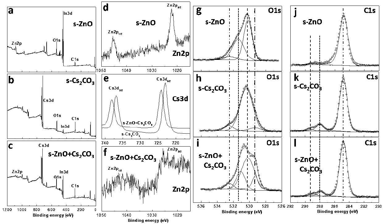
[0031] (1), preparation of cesium carbonate-ethanol solution: 99.99% cesium carbonate powder is added in 99.7% ethanol solution, and continue heating at 100 ℃ until described cesium carbonate powder dissolves completely, and the obtained concentration is 2-8% cesium carbonate-ethanol solution.

[0032] (2) Preparation of zinc oxide-methanol solution: dissolving 99.5% zinc oxide nanopowder in 99.9% methanol to prepare a zinc oxide-methanol solution with a concentration of 0.2-0.4%.

[0033] (3) Preparation of mixed solution: mix zinc oxide-methanol solution and cesium carbonate-ethanol solution with a weight ratio of 1-2:2-1 to prepare the mixed solution.

[0034] (4), ITO transparent cathode treatment: place the ITO coated glass sheet in an ultrasonic cleaner with an ultrasonic frequency of 40KHz and add distilled water for ultrasonication for 10-15m...

Embodiment 1

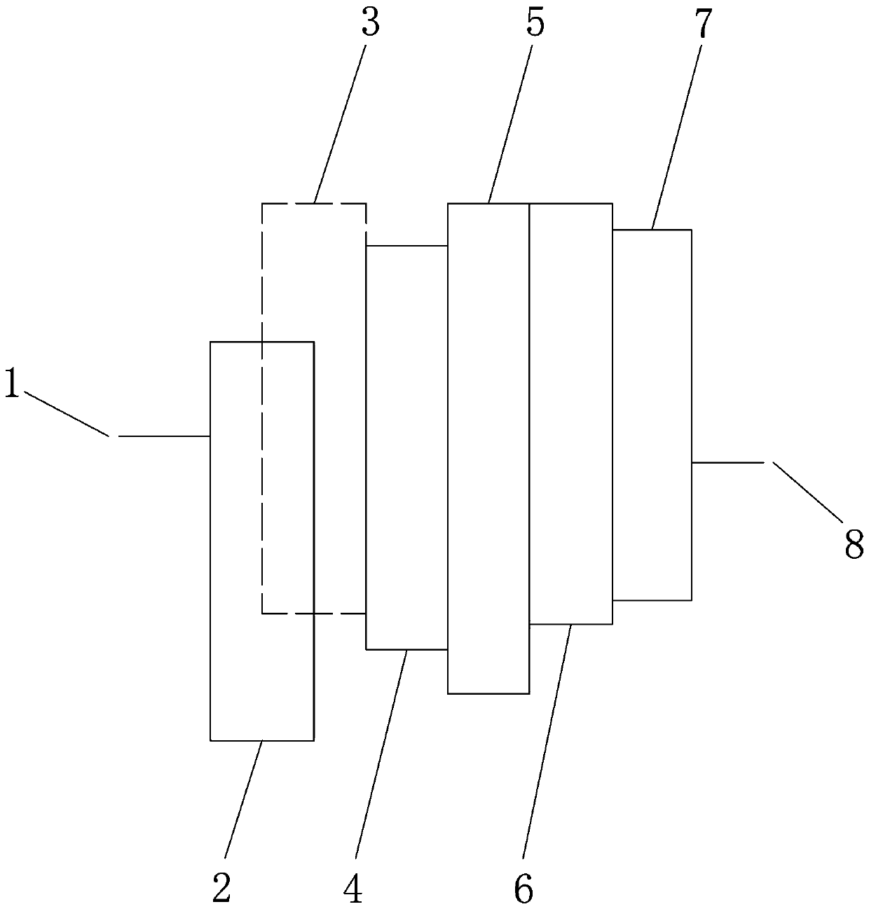
[0039] Example 1: ITO / s-Cs 2 CO 3 (2%) / BPhen(30nm) / TAZ(25nm) / CBP(100nm) / MoO 3 (5nm) / Al(200nm).

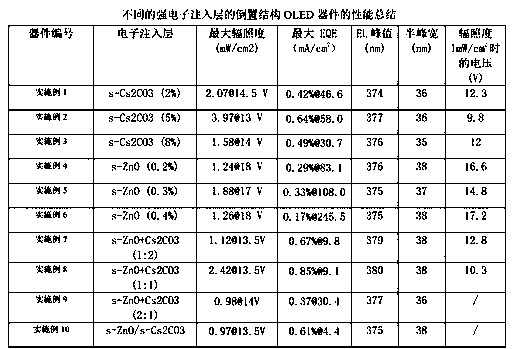
[0040]The following examples are the same as Example 1 except for the data of the strong electron injection layer.

Embodiment 2

[0041] Example 2: ITO / s-Cs 2 CO 3 (5%) / BPhen / TAZ / CBP / MoO 3 / Al;


PUM

PropertyMeasurementUnit
thicknessaaaaaaaaaa
thicknessaaaaaaaaaa
thicknessaaaaaaaaaa

Abstract

The invention discloses an inverted structure OLED device based on a strong electron injection layer and a manufacturing method thereof. The inverted structure OLED device comprises an ITO transparentcathode, a strong electron injection layer, a BPhen electron transport layer, a TAZ light-emitting layer, a CBP hole transport layer, a molybdenum trioxide hole injection layer and an Al anode from left to right. The strong electron injection layer comprises one or two of a zinc oxide layer and a cesium carbonate layer or a zinc oxide-cesium carbonate layer. The manufacturing method comprises thesteps of preparation of a cesium carbonate-ethanol solution and a zinc oxide-methanol solution, preparation of a mixed solution, treatment of the ITO transparent cathode and preparation of the inverted-structure OLED device. In the invention, cesium carbonate and zinc oxide are preferably selected to be compounded so as to serve as the strong electron injection layer; based on a TAZ light emitting layer, the OLED device shows excellent short wavelength emission, a maximum radiance is 2.42 mW/cm<2>, EQE is 0.85%, working durability is improved, and XPS analysis shows that s-ZnO+Cs2CO3 shows excellent electronic performance and is beneficial to electron injection so that electro-optical performance of the OLED device with the inverted structure is improved.

Description

technical field [0001] The invention relates to an ultraviolet organic light-emitting device, in particular to an OLED device and a preparation method thereof. Background technique [0002] In order to be compatible with the manufacturing process of OLED devices, the existing strong electron injection layers are mostly made from active alkali metals Ca, Ba, Cs, Li, Al, organic molecules pentacene and Liq, inorganic compounds LiF, CsF, Li 2 CO 3 and MoS 2 The thermal evaporation in the medium consumes more energy, the cost is higher, and the manufacturing demand that can be met is narrow. Contents of the invention [0003] In order to overcome the shortcomings of the prior art, the invention provides an OLED device with an inverted structure based on a strong electron injection layer and a preparation method thereof. [0004] The technical solution adopted by the present invention to solve its technical problems is: [0005] An OLED device with an inverted structure bas...

Claims


Application Information

Patent Timeline
Patent Type & Authority Applications(China)
IPC IPC(8): H01L51/54H01L51/50H01L51/56
CPCH10K50/171H10K2102/00H10K2102/321H10K71/00
Inventor 张小文徐凯王立惠卢宗柳刘黎明王红航
Owner GUILIN UNIV OF ELECTRONIC TECH
Why Eureka
Try Eureka