Epitaxial wafer, preparation method of epitaxial wafer, and light-emitting diode

A technology of light-emitting diodes and epitaxial wafers, applied in semiconductor devices, electrical components, circuits, etc., can solve the problems of low luminous efficiency of epitaxial wafers, achieve the effects of reducing built-in electric field, reducing overflow rate, and improving radiation recombination efficiency

Active Publication Date: 2022-07-22
JIANGXI ZHAO CHI SEMICON CO LTD
View PDF7 Cites 0 Cited by
  • Summary
  • Abstract
  • Description
  • Claims
  • Application Information

AI Technical Summary

Problems solved by technology

[0005] In view of this, the object of the present invention is to provide an epitaxial wafer, a preparation method of the epitaxial wafer and a light-emitting diode, aiming at solving the problem of low luminous efficiency of the epitaxial wafer in the prior art

Method used


Image

  • Epitaxial wafer, preparation method of epitaxial wafer, and light-emitting diode
  • Epitaxial wafer, preparation method of epitaxial wafer, and light-emitting diode
  • Epitaxial wafer, preparation method of epitaxial wafer, and light-emitting diode

Examples


Embodiment 1

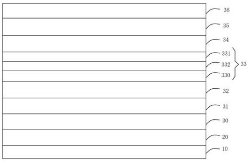
[0029] see figure 1 , shows the epitaxial wafer proposed in the first embodiment of the present invention, and the epitaxial wafer includes:

[0030] Substrate 10, AlN buffer layer 20 epitaxially grown on the substrate in sequence, undoped AlGaN layer 30, N-type doped AlGaN layer 31, multiple quantum well layer 32, composite transition layer 33, AlGaN electron blocking layer 34, P-type doped AlGaN layer 35 and AlGaN contact layer 36 .

[0031] The composite transition layer 33 includes an N-type doped AlGaN sub-layer 330 , an undoped AlGaN sub-layer 332 and a P-type doped AlGaN sub-layer 331 sequentially stacked on the multiple quantum well layer 32 .

[0032] It can be understood that by inserting a composite transition layer 33 between the multiple quantum well layer 32 and the AlGaN electron blocking layer 34, and using the P-type doped AlGaN sublayer 331 in the composite transition layer 33 to contact the AlGaN electron blocking layer 34, It alleviates the serious downwa...

Embodiment 2

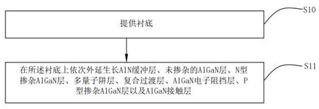
[0043] see figure 2 , is the epitaxial wafer preparation method proposed in the second embodiment of the present invention, the epitaxial wafer preparation method is used for preparing the epitaxial wafer proposed in the above-mentioned first embodiment, and the epitaxial wafer preparation method includes steps S10 to S11 .

[0044] Step S10, providing a substrate.

[0045] Specifically, in this embodiment, the substrate is a sapphire substrate.

[0046] Step S11, epitaxially growing an AlN buffer layer, an undoped AlGaN layer, an N-type doped AlGaN layer, a multiple quantum well layer, a composite transition layer, an AlGaN electron blocking layer, and a P-type doped AlGaN layer on the substrate in sequence and AlGaN contact layers.

Embodiment approach

[0047] More specifically, in order to clearly understand the specific implementation process of the present invention, the specific growth process of the epitaxial wafer is described in detail below, which is an embodiment of the present invention, but the growth process of the epitaxial wafer of the present invention is not limited to this, and It does not constitute a limitation of the present invention.

[0048] An AlN buffer layer was grown using PVD on the substrate. Among them, the growth temperature is 400°C-650°C, the sputtering power is 2000W-4000W, the pressure is 1 Torr-10 Torr, and the growth thickness is 15nm-50nm.

[0049] The buffer layer is annealed in-situ under a hydrogen atmosphere in MOCVD. Among them, the temperature is 1000°C-1200°C, the pressure range is 150 Torr-500 Torr, and the time is between 5 minutes and 10 minutes. After the annealing is completed, the temperature is adjusted to 1050°C-1200°C, and an undoped AlGaN layer with a thickness of 1.0 t...


PUM

PropertyMeasurementUnit
thicknessaaaaaaaaaa
thicknessaaaaaaaaaa
thicknessaaaaaaaaaa

Abstract

The invention provides an epitaxial wafer, a method for preparing the epitaxial wafer, and a light-emitting diode. The epitaxial wafer includes a substrate, and further includes a multiple quantum well layer, a composite transition layer and an AlGaN electron blocking layer sequentially stacked on the substrate; wherein , the composite transition layer includes an N-type doped AlGaN sub-layer, an undoped AlGaN sub-layer and a P-type doped AlGaN sub-layer sequentially stacked on the multiple quantum well layer, the N-type doped AlGaN sub-layer The dopant is Si, and the Si doping concentration is 1*10 17 / cm 3 ~1*10 18 / cm 3 , the Si doping concentration of the N-type doped AlGaN sublayer gradually decreases from one end close to the multiple quantum well layer to the other end. The invention solves the problem of low luminous efficiency of the epitaxial wafer in the prior art.

Description

technical field [0001] The invention relates to the technical field of semiconductors, in particular to an epitaxial wafer, a method for preparing the epitaxial wafer and a light emitting diode. Background technique [0002] In the past ten years, AlGaN materials have attracted much attention due to their huge application potential in ultraviolet optoelectronic devices. Ultraviolet LEDs have the characteristics of high photon energy, short wavelength, small size, low power consumption, long life, and environmental friendliness. Color rendering index white light lighting, high-density optical data storage, sensors, lithography, air purification, environmental protection and other fields have a wide range of applications. [0003] However, the development of AlGaN-based UV LEDs faces many technical difficulties, such as the small effective mass of electrons and high mobility, which leads to many electrons easily overflowing through the quantum well and overflowing to the P lay...

Claims


Application Information

Patent Timeline
Patent Type & Authority Patents(China)
IPC IPC(8): H01L33/14H01L33/02H01L33/00
CPCH01L33/025H01L33/14H01L33/007
Inventor 刘春杨胡加辉吕蒙普金从龙
Owner JIANGXI ZHAO CHI SEMICON CO LTD
Why Eureka
Try Eureka