

Single crystal semiconductor material processing equipment and use method thereof
A single crystal semiconductor and material processing technology, applied in the direction of using ultrasonic/sonic/infrasonic waves, measuring devices, instruments, etc., can solve the problem of high fragmentation rate, achieve the effect of increasing yield, high work efficiency, and avoiding waste of resources
- Summary
- Abstract
- Description
- Claims
- Application Information
AI Technical Summary
Problems solved by technology
Method used
Image

Examples
Embodiment Construction
[0033] The following will clearly and completely describe the technical solutions in the embodiments of the present invention with reference to the accompanying drawings in the embodiments of the present invention. Obviously, the described embodiments are only some, not all, embodiments of the present invention. Based on the embodiments of the present invention, all other embodiments obtained by persons of ordinary skill in the art without making creative efforts belong to the protection scope of the present invention.
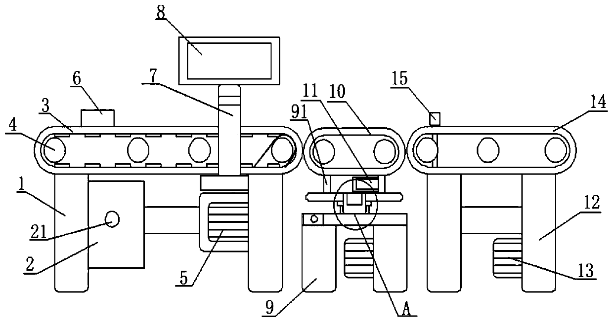
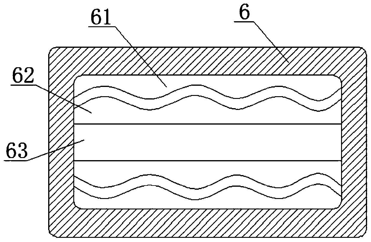
[0034] In conjunction with the accompanying drawings, a control box 2 is installed on one side of the lower part of the frame body 1; a conveyor belt 3 is installed on the upper end of the frame body 1, and a feeding box 6 is placed on the surface of the conveyor belt 3; Transmission device 4, the periphery of transmission device 4 at one end forms transmission connection with the output shaft end of first motor 5 through a transmission chain, wherein the shell...
PUM
 Abstract
Description
Claims
Application Information