OLED display substrate, manufacturing method thereof and display device

A technology for display substrates and manufacturing methods, which is applied in semiconductor/solid-state device manufacturing, electrical components, electric solid-state devices, etc., can solve the problems of low pixel aperture ratio and limit the size of pixel opening area, so as to improve the pixel aperture ratio and increase the area effect

Inactive Publication Date: 2020-06-05
HEFEI XINSHENG OPTOELECTRONICS TECH CO LTD +1
View PDF6 Cites 3 Cited by
  • Summary
  • Abstract
  • Description
  • Claims
  • Application Information

AI Technical Summary

Problems solved by technology

[0003] In OLED display devices, after the passivation layer is formed, a flat layer will be formed, and subsequent film layers such as anodes will be made on the flat layer. The flat layer can ensure the uniformity of subsequent evaporation of luminescent materials or printing of luminescent materials, thereby ensuring However, due to the pits at the anode via holes, in order to ensure the uniformity of the subsequent evaporation of luminescent materials or printing of luminescent materials, the pixel opening area needs to avoid the anode via holes, which greatly limits the size of the pixel opening area. Low pixel aperture ratio

Method used


Image

  • OLED display substrate, manufacturing method thereof and display device
  • OLED display substrate, manufacturing method thereof and display device
  • OLED display substrate, manufacturing method thereof and display device

Examples


Embodiment Construction

[0051] In order to make the technical problems, technical solutions and advantages to be solved by the embodiments of the present invention clearer, the following will describe in detail with reference to the drawings and specific embodiments.

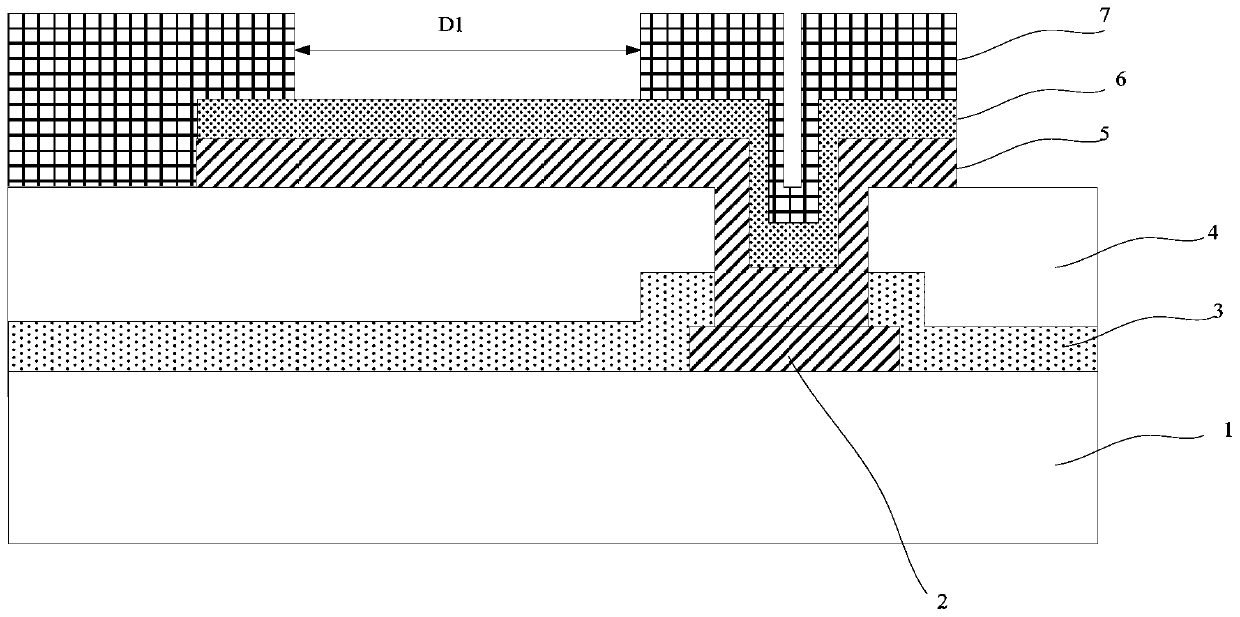
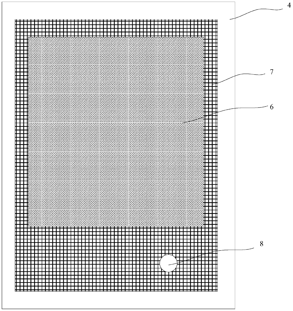
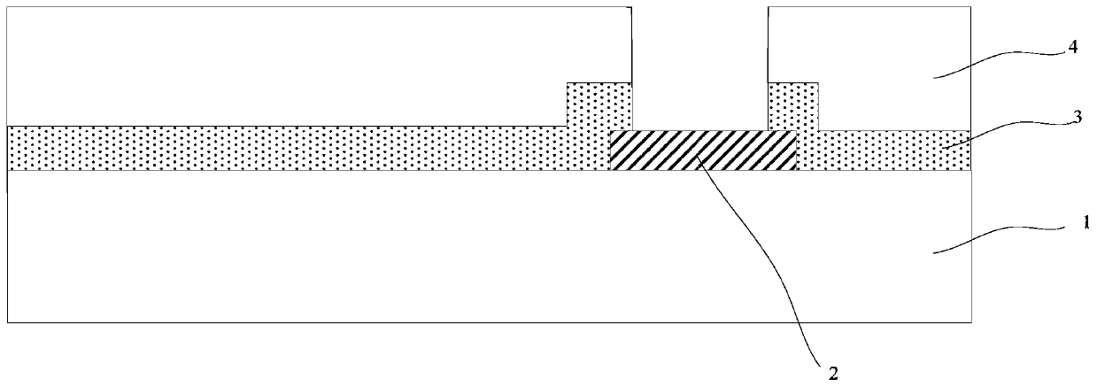
[0052] figure 1 It is a schematic cross-sectional view of a related art OLED display substrate, figure 2 It is a schematic diagram of a pixel area of ​​a related art OLED display substrate, such as figure 1 and figure 2 As shown, a passivation layer 3 and a flat layer 4 are provided on the side of the driving thin film transistor away from the substrate 1, and the anode is connected to the output electrode 2 of the driving thin film transistor through the anode via hole 8 passing through the passivation layer 3 and the flat layer 4, The anode includes a first anode pattern 5 and a second anode pattern 6 which are stacked, and the figure 1 It can be seen that there are pits at the anode via holes, in order to ensure the uniformity ...


PUM


Abstract

The invention provides an OLED display substrate, a manufacturing method thereof and a display device, and belongs to the technical field of display. The OLED display substrate comprises a driving thin film transistor, an anode, a light-emitting layer and a cathode which are located on a substrate body. An insulating layer is arranged between the anode and the driving thin film transistor in a spaced mode, the anode is connected with an output electrode of the driving thin film transistor through an anode via hole penetrating through the insulating layer, and the segment difference of the surface of the side, away from the underlayer substrate, of the anode is smaller than a threshold value. According to the technical scheme of the invention, the pixel aperture opening ratio of an OLED display product can be improved.

Description

technical field [0001] The invention relates to the field of display technology, in particular to an OLED display substrate, a manufacturing method thereof, and a display device. Background technique [0002] OLED (Organic Light Emitting Diode) display devices have gradually become the mainstream of the display industry due to their advantages of high contrast and self-illumination. [0003] In OLED display devices, after the passivation layer is formed, a flat layer will be formed, and subsequent film layers such as anodes will be made on the flat layer. The flat layer can ensure the uniformity of subsequent evaporation of luminescent materials or printing of luminescent materials, thereby ensuring However, due to the pits at the anode via holes, in order to ensure the uniformity of the subsequent evaporation of luminescent materials or printing of luminescent materials, the pixel opening area needs to avoid the anode via holes, which greatly limits the size of the pixel op...

Claims


Application Information

Patent Timeline
Patent Type & Authority Applications(China)
IPC IPC(8): H01L51/52H01L27/32H01L21/77
CPCH10K59/124H10K59/131H10K50/813H10K59/1201
Inventor 张扬周斌丁远奎宋嘉文罗志文王庆贺
Owner HEFEI XINSHENG OPTOELECTRONICS TECH CO LTD
Why Eureka
Try Eureka