Gallium nitride-based vertical structure light emitting diode with current blocking layer and manufacturing method thereof

A technology of light-emitting diodes and current blocking layers, applied in circuits, electrical components, semiconductor devices, etc., can solve the problems of light-emitting layer falling off, bonding failure, and large difference in thermal expansion coefficient, etc., achieve good light reflection, and realize current distribution adjustment Effect

Inactive Publication Date: 2020-06-09
西安唐晶量子科技有限公司
View PDF6 Cites 0 Cited by
  • Summary
  • Abstract
  • Description
  • Claims
  • Application Information

AI Technical Summary

Problems solved by technology

The CN200810237845 patent proposes a solution that uses a diffusion barrier layer in a local area and Ag to degrade through high-temperature annealing. When this solution is implemented, it must be ensured that Au will diffuse to the surface of the current blocking area, and the reflectivity of Au is lower than that of Ag, resulting in current blocking. Regional reflectivity decreases, reducing light extraction efficiency
The published application number 201811636723.5 is similar to the present invention, but...

Method used


Image

  • Gallium nitride-based vertical structure light emitting diode with current blocking layer and manufacturing method thereof
  • Gallium nitride-based vertical structure light emitting diode with current blocking layer and manufacturing method thereof
  • Gallium nitride-based vertical structure light emitting diode with current blocking layer and manufacturing method thereof

Examples


Embodiment Construction

[0044] The present invention will be further described in detail below in conjunction with specific embodiments, which are explanations of the present invention rather than limitations.

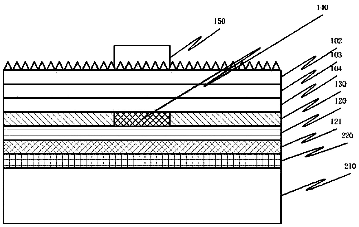
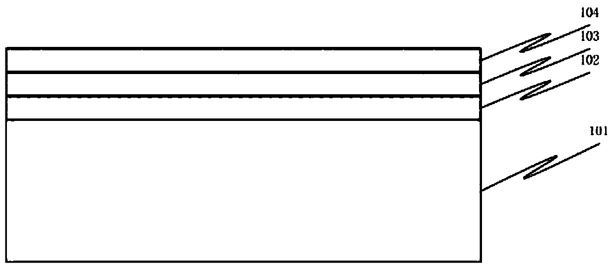
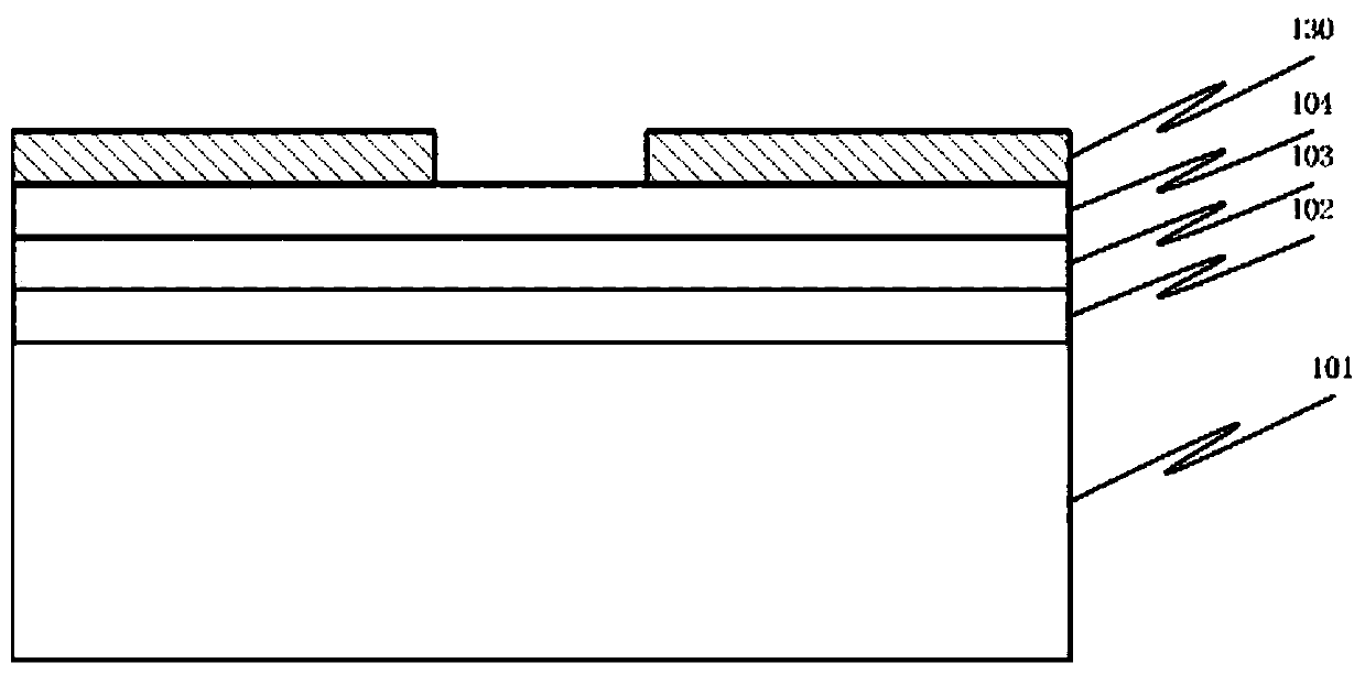
[0045] The main purpose of the present invention is to provide a vertical GaN-based light-emitting diode, the specific structure is as follows figure 1 As shown, the present invention uses Al metal as the current blocking layer of the vertical GaN-based light-emitting diode. The use of Al metal as the current blocking layer is mainly based on the following reasons: 1. When the heat treatment temperature is lower than 320 ° C, the Al metal forms a non-ohmic contact with the p-GaN surface, so the Al metal can block the current; 2. 1. Pressure and heating are required during the bonding process. When the two are combined, the thermal expansion coefficients of Ag and Al are 19.5E-6 / K and 23.2E-6 / K, respectively, which are close in size. In addition, Al and p-GaN have good adhesion , so it is eas...


PUM

PropertyMeasurementUnit
Thicknessaaaaaaaaaa

Abstract

The invention discloses a gallium nitride-based vertical structure light-emitting diode with a current blocking layer, which comprises a conductive substrate located at a bottom layer, a second welding layer located on the surface of the conductive substrate, a first welding layer located on the surface of the second welding layer, a diffusion barrier layer located on the surface of the first welding layer, a nickel-silver reflecting layer located on the surface of the diffusion barrier layer, an Al layer located on the surface of the diffusion barrier layer, a gallium nitride-based light-emitting epitaxial layer located on the surfaces of the nickel-silver reflecting layer and the Al layer and a n electrode located on the surface of the light-emitting epitaxial layer, wherein the Al metallayer is located in a projection area below the n electrode, the Al metal layer serves as a current blocking layer to change current injection, and the light-emitting efficiency is improved.

Description

technical field [0001] The invention belongs to the field of semiconductors, and in particular relates to a gallium nitride-based vertical structure light-emitting diode with a current blocking layer and a manufacturing method thereof. Background technique [0002] In recent years, vertical structure LEDs have won a place in the market because of their good performance under high current injection. Vertical structure LEDs remove the growth substrate and transfer the gallium nitride-based light-emitting layer to a secondary substrate with better thermal conductivity. , which improves its heat dissipation performance under high current conditions. In addition, because its electrodes are in an up-and-down structure, there is no current crowding effect. Compared with traditional formal structure LEDs, vertical structure LEDs have obvious advantages under high current conditions. Therefore, its in High-power fields, such as high-brightness torches, are widely used. [0003] Beca...

Claims


Application Information

Patent Timeline
IPC IPC(8): H01L33/40H01L33/00
CPCH01L33/0066H01L33/0075H01L33/40H01L33/405
Inventor 龚平吴旗召
Owner 西安唐晶量子科技有限公司
Why Eureka
Try Eureka