Power factor correction circuit and assembly and online uninterruptible power supply comprising same
A power factor correction and circuit technology, applied in output power conversion devices, electrical components, circuit devices, etc., can solve the problem of high cost and loss of low-voltage AC transmission lines, reduce the economy and efficiency of power distribution systems, and increase equipment footprint. and other problems, to achieve the effect of low cost, online service and small size
Pending Publication Date: 2020-06-12
EATON INTELLIGENT POWER LIMITED
0 Cites 0 Cited by
AI-Extracted Technical Summary
Problems solved by technology
Under high-power loads, the cost and loss of low-voltage AC transmission lines are large, which reduces the economy and efficiency of the entire power distribution system
In addition, it is necessary to increase the ...
Method used
Control device (not shown in Fig. 2) controls full bridge pulse width modulation rectifier 211,221 work respectively, and the voltage that the metal oxide field effect transistor in each full bridge pulse width modulation rectifier bears will reduce, thus The risk of failure of the power factor correction component 2 is reduced, and at the same time, its input terminal can receive medium-voltage alternating current with a relatively large voltage value. The efficiency of medium voltage alternating current is increased because the transmission efficiency of medium voltage alternating current is higher than that of low voltage alternating current.
In the online uninterruptible power supply 8 of the present invention, the three power factor correction components 83 are the same, and the three-phase inverters 821 and 822 are the same, which are suitable for mass production, convenient for replacement and maintenance, and convenient for operators to assemble and wiring to avoid misassembly.
[0063] In addition to reducing the voltage, the transformer Tr2 also isolates the medium-voltage grid connected to the primary side and the low-voltage alternating current connected to the secondary side, thereby improving safety.
[0084] The bidirectional DC-DC conversion circuit 7111 includes a metal oxide half field effect transistor T711 with an antiparallel diode D711, a metal oxide half field effect transistor T712 with an antiparallel diode D712, an inductor L71 and a capacitor C...
Abstract
The invention provides a power factor correction circuit and assembly and an online uninterruptible power supply comprising the same, the power factor correction circuit comprises a pulse width modulation rectifier and an isolated DC-DC converter, and the output end of the pulse width modulation rectifier is connected to the input end of the isolated DC-DC converter. The power factor correction assembly comprises a plurality of power factor correction circuits, the input ends of pulse width modulation rectifiers in the plurality of power factor correction circuits are connected in series, andthe output ends of isolated DC-DC converters in the plurality of power factor correction circuits are connected in parallel. The power factor correction assembly is free of an industrial frequency transformer, small in size and low in cost, and the working reliability is improved.
Application Domain
Ac-dc conversion without reversalEfficient power electronics conversion +3
Technology Topic
Power factor correctorDc converter +7
Image
Examples
- Experimental program(1)
Example Embodiment
[0056] In order to make the object, technical solution and advantages of the present invention clearer, the present invention will be further described in detail below through specific embodiments in conjunction with the accompanying drawings.
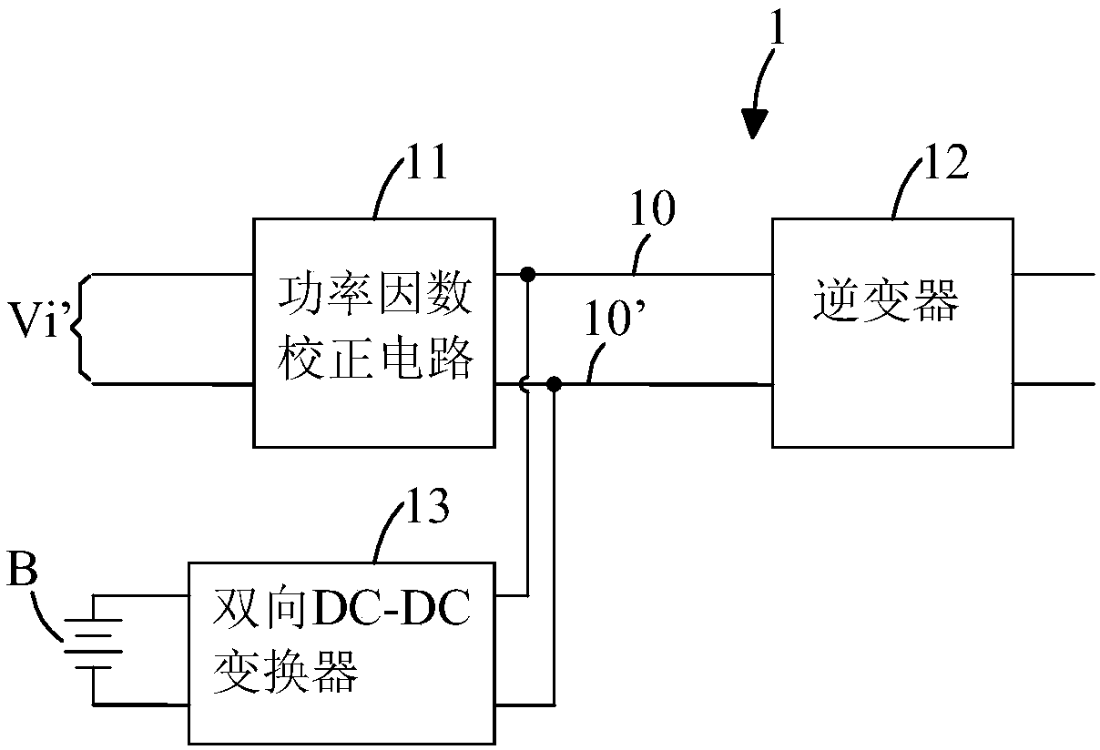
[0057] figure 2 is a circuit diagram of a power factor correction assembly according to a first embodiment of the present invention. like figure 2 As shown, the power factor correction component 2 includes a power factor correction circuit 21 and a power factor correction circuit 22. The input terminals of the power factor correction circuits 21 and 22 are connected in series and then connected to a medium-voltage alternating current Vi (for example, 10 kV), and the output terminal The parallel connection is between the positive DC bus 20 and the negative DC bus 20'.
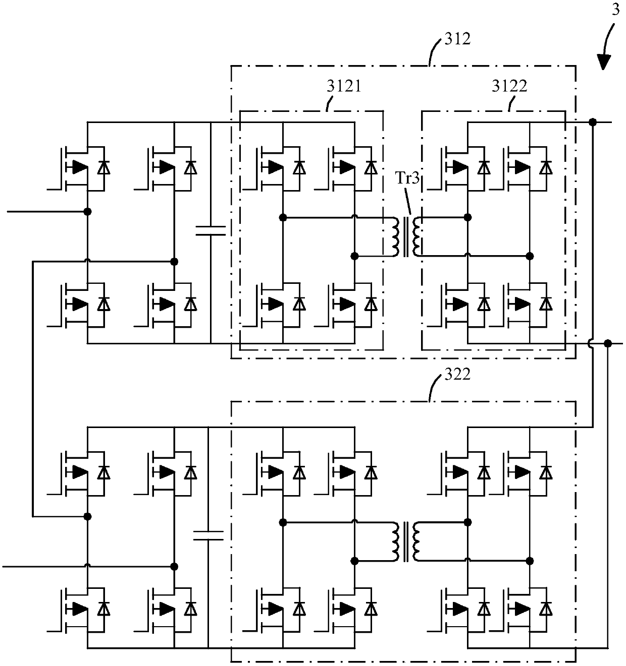
[0058] The power factor correction circuit 21 includes a cascaded full bridge pulse width modulation rectifier 211 and an isolated DC-DC converter 212 . The full-bridge pulse width modulation rectifier 211 includes four MOSFETs and a capacitor C21. Among them, four metal-oxide-semiconductor field-effect transistors are provided with pulse width modulation signals, so that the current and voltage of the alternating current at the input end of the full-bridge pulse width modulation rectifier 211 are in phase, so that the power factor of the alternating current is close to 1, and at the same time, it is obtained on the capacitor C21 DC power required.
[0059] The isolated DC-DC converter 212 includes a half-bridge inverter 2121 , a transformer Tr2 and a half-bridge pulse width modulation rectifier 2122 . The input end of the half-bridge inverter 2121 is connected to the output end of the full-bridge PWM rectifier 211, and its output end is connected to the primary side of the transformer Tr2. The input terminal of the half-bridge PWM rectifier 2122 is connected to the secondary side of the transformer Tr2, and its output terminal is connected to (or used as) the positive DC bus 20 and the negative DC bus 20'.
[0060] The half-bridge inverter 2121 is controlled to convert the direct current on the capacitor C21 into high-frequency alternating current and output it to the primary side of the transformer Tr2, so as to obtain high-frequency alternating current at the secondary side of the transformer Tr2. The half-bridge PWM rectifier 2122 is controlled to convert the AC power on the secondary side of the transformer Tr2 into DC power and transmit it to the positive and negative DC bus bars 20, 20'.
[0061] The power factor correction circuit 22 has the same circuit structure as the power factor correction circuit 21 , and it also includes a cascaded full-bridge PWM rectifier 221 and an isolated DC-DC converter 222 . Wherein the input end of the full-bridge PWM rectifier 221 is connected in series with the input end of the full-bridge PWM rectifier 211, that is, one input terminal of the full-bridge PWM rectifier 221 is connected to the full-bridge PWM rectifier 211 One input terminal, the other input terminal of the full bridge pulse width modulation rectifier 221 and the other input terminal of the full bridge pulse width modulation rectifier 211 are connected to the alternating current Vi; the output terminal of the isolated DC-DC converter 222 is connected to the isolated DC- The output terminals of the DC converter 212 are connected in parallel between the positive DC bus 20 and the negative DC bus 20'.
[0062] control device ( figure 2 (not shown) control the operation of the full-bridge PWM rectifiers 211 and 221 respectively, and the voltage borne by the metal-oxide-semiconductor field-effect transistors in each full-bridge PWM rectifier will be reduced, thereby reducing the occurrence of the power factor correction component 2 The risk of failure, while its input can receive medium-voltage AC power with a large voltage value. The efficiency of medium voltage alternating current is increased because the transmission efficiency of medium voltage alternating current is higher than that of low voltage alternating current.
[0063] In addition to reducing the voltage, the transformer Tr2 also isolates the medium-voltage grid connected to the primary side and the low-voltage alternating current connected to the secondary side, thereby improving safety.
[0064] At the same time, since the magnetic core of the transformer Tr2 provides a magnetic circuit for the alternating magnetic field generated by high-frequency alternating current, the selection of a very small magnetic core will not cause its magnetic saturation, that is, a small-sized high-frequency transformer can be selected, such as the selection of the operating frequency High frequency transformers greater than 10kHz. Compared with large-volume power frequency transformers, the sum of the volumes of all high-frequency transformers in the power factor correction component 2 in this embodiment is much smaller than the volume of one power frequency transformer, and a cabinet with a smaller volume can be selected; and this In the process of connecting and assembling multiple power factor correction circuits in the power factor correction assembly 2 of the embodiment, the distance between the circuit modules can be smaller, and the entire cabinet can be designed more compactly.
[0065] In other embodiments of the present invention, the power factor correction assembly 2 includes more than two power factor correction circuits. In practical applications, an appropriate number of power factor correction circuits is selected according to the voltage value of the alternating current Vi and the withstand voltage value of the metal oxide semiconductor field effect transistor. For example, when the alternating current Vi is a medium-voltage alternating current, select a power factor correction circuit whose number is far more than two, connect the input ends of each power factor correction circuit in series and then connect it to the medium-voltage alternating current, and connect the input terminals of each power factor correction circuit to the medium-voltage alternating current. The output terminals are connected in parallel between the positive DC bus and the negative DC bus. When the number of power factor correction circuits increases, the input terminal of the power factor correction component 2 can receive alternating current with a larger voltage value.
[0066] image 3 is a circuit diagram of a power factor correction assembly according to a second embodiment of the present invention. like image 3 As shown, the power factor correction component 3 with figure 2 The power factor correction assembly 2 is basically the same, the difference is that the isolated DC-DC converter 312 includes a full-bridge inverter 3121 connected to the primary side of the transformer Tr3, and a full-bridge inverter 3121 connected to the secondary side of the transformer Tr3 Wide modulation rectifier 3122. The isolated DC-DC converter 322 is the same as the isolated DC-DC converter 312 and will not be repeated here.
[0067] Figure 4 is a circuit diagram of a power factor correction assembly according to a third embodiment of the present invention. like Figure 4 As shown, the power factor correction component 4 with figure 2 The power factor correction assembly 2 is basically the same, except that the isolated DC-DC converter 412 includes a bridge rectifier circuit 4122 connected to the secondary side of the transformer Tr4. The isolated DC-DC converter 422 is the same as the isolated DC-DC converter 412 and will not be repeated here.
[0068] Figure 5 is a circuit diagram of a power factor correction assembly according to a fourth embodiment of the present invention. like Figure 5 As shown, the power factor correction component 5 with figure 2 The power factor correction assembly 2 is basically the same, the difference is that the power factor correction circuit 51 includes a cascaded half-bridge pulse width modulation rectifier 511 and an isolated DC-DC converter 512, wherein the isolated DC-DC converter 512 includes a transformer The primary side of Tr5 is connected to a full-bridge inverter 5121. The power factor correction circuit 52 is the same as the power factor correction circuit 51 and will not be repeated here.
[0069] Image 6 is a circuit diagram of a power factor correction component in a normal working state according to the fifth embodiment of the present invention. like Image 6 As shown, the power factor correction component 6 includes two identical power factor correction circuits 61 and 62, and the following only takes the power factor correction circuit 61 as an example for illustration.
[0070] power factor correction circuit 61 with figure 2 The power factor correction circuit 21 in is basically the same, the difference is that it also includes a switch S61 and a fuse F61 connected in series with one input terminal of the full-bridge pulse width modulation rectifier 611, a switch S62 and a fuse F61 connected in series with the other input terminal and a fuse F63 and switch S63 connected in series to one output terminal of the isolated DC-DC converter 612, and a fuse F64 and switch S64 connected in series to the other output terminal thereof.
[0071] The power factor correction component 6 also includes a switch S65 and a switch S65', the switch S65 is connected between the input terminals of the power factor correction circuit 61, and the switch S65' is connected between the input terminals of the power factor correction circuit 62.
[0072] like Image 6 As shown, under normal working conditions, the control device ( Image 6 Not shown) control switch S65 and switch S65' to be in an off state, and control switches S61, S62, S63 and S64 in the power factor correction circuit 61 to be in an on state, and control switch S61 in the power factor correction circuit 62 ', S62', S63' and S64' are all in the conduction state. At this time, the input ends of the power factor correction circuit 61 and the power factor correction circuit 62 are connected in series, and the output ends are connected in parallel between the positive DC bus 60 and the negative DC bus 60', and the power factor correction component 6 and figure 2 The equivalent circuit of the shown power factor correction component 2 is the same, and its working mode will not be repeated here.
[0073] Figure 7 Yes Image 6 Circuit diagram when one of the power factor correction circuits in the power factor correction assembly shown fails. like Figure 7 As shown, when the circuit on the primary side of the transformer Tr6 in the power factor correction circuit 61 fails, the fuse F61 and the fuse F62 will be blown at this time; or when the circuit on the secondary side of the transformer Tr6 fails, the fuse F63 and fuse F64 will be blown. Then the switch S65 is controlled to be turned on to short-circuit the input terminal of the power factor correction circuit 61 . Then the control switches S61, S62, S63 and S64 are turned off. At this time, since the full-bridge pulse width modulation rectifier 611 is short-circuited by the switch S65 that is turned on, the alternating current Vi is connected to the input terminal of the power factor correction circuit 62 through the switch S65 that is turned on, so the operation of the power factor correction circuit 62 is not affected ( In other words, the normal operation of the non-faulty power factor correction circuits in the power factor correction components is not affected).
[0074] After the switches S61 , S62 , S63 and S64 are turned off, maintenance personnel can remove the faulty power factor correction circuit 61 and then reconnect a new power factor correction circuit 61 to the power factor correction component 6 . Next, the control switches S61, S62, S63 and S64 are closed, and then the control switch S65 is opened. At this time, the input terminal of the power factor correction circuit 61 is connected in series with the input terminal of the power factor correction circuit 62, and the output of the power factor correction circuit 61 terminal and the output terminal of the power factor correction circuit 62 are connected in parallel between the positive and negative DC buses 60, 60'.
[0075] It can be seen that even if any power factor correction circuit in the power factor correction assembly 6 fails, the maintenance personnel can replace the faulty power factor correction circuit while the power factor correction assembly 6 is still working, so the power factor The correction component 6 realizes online service and hot plug function.
[0076] In other embodiments of the present invention, the Image 6 The shown switches S61-S65 and fuses F61-F64 are connected to each power factor correction circuit in the power factor correction assembly 3, 4 or 5.
[0077]In other embodiments of the present invention, other rectification devices may also be used to replace the half-bridge PWM rectifier 2122 , the full-bridge PWM rectifier 3122 or the bridge rectifier circuit 4122 in the above embodiments.
[0078] In other embodiments of the present invention, the power factor correction component includes more than two power factor correction circuits, and when one or more power factor correction circuits in the power factor correction component fail, the power factor correction component can still be guaranteed to work , greatly improving the reliability of work. It is also possible to replace a failed power factor correction circuit or circuits without interrupting the operation of the power factor correction components.
[0079] The power factor correction components 2, 3, 4, 5, and 6 in the above embodiments of the present invention all include the same power factor correction circuit, which is suitable for mass production, facilitates the replacement of faulty power factor correction circuits, and can effectively avoid wiring failures and misassembly, and the control process of the same power factor correction circuit by the control device is simple.
[0080] Figure 8 It is a circuit diagram of the online uninterruptible power supply according to the first embodiment of the present invention. like Figure 8 As shown, the on-line uninterruptible power supply includes a power factor correction component 7 , a bidirectional DC-DC converter component 71 , and an inverter component 72 .
[0081] power factor correction components 7 with Image 6 The power factor correction components 6 shown are the same and will not be repeated here. A bidirectional DC-DC converter assembly 71 is connected between the rechargeable battery B and the positive and negative DC bus bars 70, 70'. The input end of the inverter assembly 72 is connected to the positive and negative DC bus bars 70, 70', and its output end is used to provide the load with an alternating current Vo.
[0082] Figure 9 Yes Figure 8 An enlarged schematic diagram of the bidirectional DC-DC converter assembly in . like Figure 9 As shown, the bidirectional DC-DC converter assembly 71 includes bidirectional DC-DC converters 711, 712 connected in parallel, that is, the bidirectional DC-DC converters 711, 712 are connected to the rechargeable battery B and the positive and negative DC bus bars 70, 70 'between.
[0083] The circuit structures of the bidirectional DC-DC converters 711 and 712 are the same, and the following only uses the bidirectional DC-DC converter 711 as an example for illustration. The bidirectional DC-DC converter 711 includes a bidirectional DC-DC conversion circuit 7111, a switch S711 and a fuse F711 connected in series with the positive terminal of the first connection end of the bidirectional DC-DC conversion circuit 7111, and a switch connected in series with the negative terminal of the first connection end of the bidirectional DC-DC conversion circuit 7111. S712, a fuse F712, and a switch S713 and a switch S714 respectively connected to the positive terminal and the negative terminal of the second connection end.
[0084] The bidirectional DC-DC conversion circuit 7111 includes a metal oxide semiconductor field effect transistor T711 with an antiparallel diode D711, a metal oxide semiconductor field effect transistor T712 with an antiparallel diode D712, an inductor L71 and a capacitor C71. Among them, the inductor L71, the metal oxide half field effect transistor T711 and the antiparallel diode D712 are connected to form a Boost circuit (or Boost boost circuit), and the metal oxide half field effect transistor T712, the antiparallel diode D711 and the inductor L71 are connected Form a Buck circuit (or Buck step-down circuit). The capacitor C71 is connected between one end of the inductor L71 and the anode of the anti-parallel diode D711, and is used to filter the high-frequency alternating current and effectively protect the rechargeable battery B.
[0085] If both bidirectional DC-DC converters 711 and 712 are normal (that is, there is no fault), in the online working mode (that is, the mains power is normal), the control device ( Figure 9 not shown) control the bidirectional DC-DC converters 711, 712 to implement step-down conversion, so as to store the electric energy on the positive and negative DC bus bars 70, 70' into the rechargeable battery B; ), control the bidirectional DC-DC converters 711, 712 to implement boost conversion, so as to store the electric energy in the rechargeable battery B into the positive and negative DC bus bars 70, 70'.
[0086] If the bidirectional DC-DC conversion circuit 7111 fails, the fuses F711 and F712 will be blown at this time, and the control device controls the switches S711, S712, S713 and S714 to be in the disconnected state. Since the bidirectional DC-DC converter 712 connected in parallel with the bidirectional DC-DC converter 711 is still working, it will not affect the discharge or charge of the rechargeable battery B. At this time, the maintenance personnel can remove the failed bidirectional DC-DC converter 711 from the bidirectional DC-DC converter assembly 71, and replace a new bidirectional DC-DC converter 711, and finally control the switches S711, S712, S713 and S714 is turned on, thereby realizing reconnecting the bidirectional DC-DC converter 711 into the bidirectional DC-DC converter component 71 .
[0087] In other embodiments of the present invention, the fuse F711 and the fuse F712 are respectively connected in series with the switches S713 and S714.
[0088] In other embodiments of the present invention, the bidirectional DC-DC converter assembly 71 includes more than 2 bidirectional DC-DC converters, and after multiple bidirectional DC-DC converters are connected in parallel, they are connected between the rechargeable battery B and the positive , Between the negative DC bus. A plurality of bidirectional DC-DC converters work at the same time, in addition to providing greater output power, it can also effectively protect the components in the bidirectional DC-DC converter assembly 71 from being damaged, reducing the risk of failure.
[0089] In other embodiments of the present invention, a separate DC-DC converter and a charger are used to replace the bidirectional DC-DC conversion circuit 7111 in the above embodiment, wherein the input terminal of the charger is connected to the output terminal of the DC-DC converter , the output terminal of the charger is connected to the input terminal of the DC-DC converter.
[0090] Figure 10 Yes Figure 8 An enlarged schematic view of the inverter assembly in , as in Figure 10 As shown, the inverter assembly 72 includes two parallel inverters 721, 722, that is, the input ends of the inverters 721, 722 are connected to the positive and negative DC bus bars 70, 70', and the output ends of the two are connected to together and provide the required AC current Vo to the load.
[0091] The circuit structures of the inverters 721 and 722 are the same, and the following only uses the inverter 721 as an example for illustration. The inverter 721 includes a full bridge inverter circuit 7211 formed by connecting four metal oxide half field effect transistors and an inductor L72, and a switch S721 connected in series between the positive input terminal of the full bridge inverter circuit 7211 and the positive DC bus 70 and fuse F721, a switch S722 and a fuse F722 connected in series between the negative input terminal of the full-bridge inverter circuit 7211 and the negative DC bus 70', and an output connected to the two output terminals of the full-bridge inverter circuit 7211 Switches S723, S724. Under normal working conditions, the switches S721, S722 and the output switches S723, S724 are all in the conduction state. The control method of the full-bridge inverter circuit 7211 is the same as that of the prior art, and will not be repeated here.
[0092] If the full-bridge inverter circuit (such as the full-bridge inverter circuit 7211) in the inverter assembly 72 breaks down, the fuses F721 and F722 will be blown at this time, and the control device ( Figure 10 Not shown) control switches S721, S722 and output switches S723, S724 are in an off state. Since other inverters in the inverter assembly 72 (for example, the inverter 722 ) are still working, it will not affect the supply of the AC power Vo to the load. At this time, maintenance personnel can remove the faulty inverter 721 and replace it with a new inverter 721. Will be rewired into the inverter assembly 72 .
[0093] The inverter assembly 72 of the present invention is not limited to being composed of two inverters connected in parallel. In other embodiments of the present invention, it can also be formed by connecting more than two inverters in parallel. When the positive and negative DC buses 70 When a larger power can be increased on , 70 ′, the inverter assembly 72 of this embodiment can not only increase the output power, but also reduce the risk of damage to each inverter.
[0094] After one or more inverters in the inverter assembly of the present invention fail, maintenance personnel can also replace the failed inverters under the condition that they continue to work and provide alternating current, thereby improving the reliability of work.
[0095] In other embodiments of the present invention, a half-bridge inverter circuit is used to replace the full-bridge inverter circuit in the inverter assembly 72 .
[0096] Figure 11 is a circuit diagram of the inverter assembly in the on-line uninterruptible power supply according to the second embodiment of the present invention. like Figure 11 As shown, the inverter assembly 72' and Figure 10 The inverter components 72 shown are basically the same, the difference is that T-shaped three-level inverters 7211' and 7221' are used to replace Figure 10 Two full-bridge inverter circuits in. The replacement method of the T-type three-level inverter that fails in the inverter assembly 72' Figure 10 The replacement method of the full-bridge inverter circuit in is the same, and will not be repeated here.
[0097] In other embodiments of the present invention, other inverters such as I-type three-level inverters are used to replace Figure 11 The T-type three-level inverters 7211', 7221' in.
[0098] Figure 12 is a circuit diagram of an on-line uninterruptible power supply according to a third embodiment of the present invention. like Figure 12 As shown, the on-line uninterruptible power supply 8 includes three identical power factor correction components 83 , a bidirectional DC-DC converter 81 and a three-phase inverter component 82 . The input ends of the three power factor correction components 83 are respectively connected to the A, B, and C three-phase medium-voltage alternating currents, and the output ends are all connected in parallel to the positive and negative DC bus bars 80, 80'. A bidirectional DC-DC converter 81 is connected between the rechargeable battery and the positive and negative DC buses 80, 80'. The input end of the three-phase inverter assembly 82 is connected to the positive and negative DC busbars 80, 80', and its output end is used to provide U, V, W three-phase low-voltage alternating current.
[0099] power factor correction assembly 83 with Image 6 The circuit structure of the power factor correction assembly 6 shown is the same, and the bidirectional DC-DC converter 81 and Figure 9 The circuit structure of the shown bidirectional DC-DC converter 71 is the same, and will not be repeated here.
[0100] Figure 13 Yes Figure 12 An enlarged schematic of the three-phase inverter assembly in . like Figure 13 As shown, the three-phase inverter assembly 82 includes two three-phase inverters 821, 822 connected in parallel, that is, the input end of the three-phase inverter 821 and the input end of the three-phase inverter 822 are connected in parallel to positive, One of the output terminals of the negative DC bus bars 80, 80' and the three-phase inverters 821, 822 is connected to the neutral line N, and the other three output terminals are connected in parallel to provide U, V, W three-phase AC power.
[0101]The circuit structures of the three-phase inverters 821 and 822 are the same, and the following only uses the three-phase inverter 821 as an example for illustration. The three-phase inverter 821 includes a three-phase four-leg inverter circuit 8211, a switch S821 and a fuse F821 connected in series between the positive DC bus 80 and the positive input terminal of the three-phase four-leg inverter circuit 8211, and a negative DC A switch S822 and a fuse F822 connected in series between the bus bar 80' and the negative input terminal of the three-phase four-leg inverter circuit 8211, and an output switch S823 respectively connected to the four output terminals of the three-phase four-leg inverter circuit 8211 , an output switch S824, an output switch S825, and an output switch S826.
[0102] In normal working condition, the control device ( Figure 13 not shown) control all the switches in the three-phase inverters 821, 822 to be turned on, and control the operation of the three-phase four-leg inverter circuit to invert the DC power between the positive and negative DC bus bars 80, 80' into three Phase alternating current, so that U, V, W three-phase low-voltage (such as 400 volts, 480 volts or 600 volts) alternating current is obtained at its output.
[0103] If the three-phase four-leg inverter circuit 8211 in the three-phase inverter 821 breaks down, the fuse F821 and the fuse F822 are blown, and the control device controls the switches S821, S822 and output switches in the three-phase inverter 821 S823, S824, S825, and S826 are disconnected. Since the three-phase inverter 822 connected in parallel with the three-phase inverter 821 is still in working condition, maintenance personnel can replace the failed three-phase inverter without affecting its supply of U, V, W three-phase low-voltage alternating current. The inverter 821 is removed and replaced with a new three-phase inverter 821. Finally, the control device controls the switches S821, S822 and the output switches S823, S824, S825, and S826 to be in a conducting state.
[0104] In the online uninterruptible power supply 8 of the present invention, the three power factor correction components 83 are the same, and the three-phase inverters 821 and 822 are the same, which are suitable for mass production, convenient for replacement and maintenance, convenient for operators to assemble and connect, and avoid misassembly.
[0105] In other embodiments of the invention, the three-phase inverter assembly 82 includes more than two three-phase inverters connected in parallel, thereby reducing the risk of failure of each of the three-phase inverters connected in parallel, and It can provide greater output power and improve power density.
[0106] In other embodiments of the present invention, a three-phase inverter circuit such as a three-phase three-leg inverter circuit, a T-type three-level three-phase inverter circuit or an I-type three-level three-phase inverter circuit may be used instead of the above-mentioned In the three-phase four-leg inverter circuit of the embodiment, correspondingly, there are three output switches connected to the output terminals of these three-phase inverter circuits.
[0107] In another embodiment of the present invention, the input end of the on-line uninterruptible power supply is connected to single-phase alternating current, and the output end thereof is used to provide three-phase alternating current.
[0108] In yet another embodiment of the present invention, the input end of the on-line uninterruptible power supply is connected to three-phase alternating current, and its output end is used to provide single-phase alternating current.
[0109] In other embodiments of the present invention, a switching transistor such as an insulated gate bipolar transistor with an antiparallel diode may also be used instead of the metal oxide semiconductor field effect transistor in the above embodiment.
[0110] Although the present invention has been described in terms of preferred embodiments, the present invention is not limited to the embodiments described herein, and various changes and changes are included without departing from the scope of the present invention.
PUM


Description & Claims & Application Information
We can also present the details of the Description, Claims and Application information to help users get a comprehensive understanding of the technical details of the patent, such as background art, summary of invention, brief description of drawings, description of embodiments, and other original content. On the other hand, users can also determine the specific scope of protection of the technology through the list of claims; as well as understand the changes in the life cycle of the technology with the presentation of the patent timeline. Login to view more.
Similar technology patents
Topological magnetic integrated converter suitable for LLC resonance series
Owner:NANJING UNIV OF AERONAUTICS & ASTRONAUTICS
Classification and recommendation of technical efficacy words
- reduce volume
- low cost
Implant release mechanism
Owner:COOK MEDICAL TECH LLC
Speed reduction box for turbine fracturing
Owner:YANTAI JEREH PETROLEUM EQUIP & TECH
Miniature and Multi-Band RF Coil Design
Owner:HONG KONG APPLIED SCI & TECH RES INST
Automatic washing and dewatering combined device of rotary type mop
Owner:上海祥美网络科技有限公司 +1
Optical imaging system
Owner:SAMSUNG ELECTRONICS CO LTD
Method, apparatus and article for microfluidic control via electrowetting, for chemical, biochemical and biological assays and the like
Owner:KECK GRADUATE INST OF APPLIED LIFE SCI
System and method for transmitting wireless digital service signals via power transmission lines
Owner:NEXTEL COMMUNICATIONS
System and method for determination of position
Owner:STEELE CHRISTIAN