Source bottle and semiconductor equipment

A source bottle and bottle cap technology is applied in the field of source bottles and semiconductor equipment, which can solve the problems that the solid powder source cannot be flattened, waste time, and the shape of the solid powder source surface cannot be determined and guaranteed, so as to solve the problem of insufficient solid source vapor concentration, The effect of increasing the steam concentration and increasing the contact area

Active Publication Date: 2020-06-16
BEIJING NAURA MICROELECTRONICS EQUIP CO LTD
View PDF6 Cites 3 Cited by
  • Summary
  • Abstract
  • Description
  • Claims
  • Application Information

AI Technical Summary

Problems solved by technology

[0005] While the solid powder source is loaded in the solid source bottle, the plane of the solid powder source may not be flat, and the solid powder source may be tilted, bumped, etc. during transportation, resulting in the uncertainty and guarantee of the shape of the solid powder source surface in the bottle, which leads to Using the same process parameters does not necessarily produce films with the same quality. Every time the source bottle is replaced, the process parameters need to be measured again, which is a waste of time, a large workload, and a long recovery time.

Method used


Image

  • Source bottle and semiconductor equipment
  • Source bottle and semiconductor equipment
  • Source bottle and semiconductor equipment

Examples


Embodiment 3

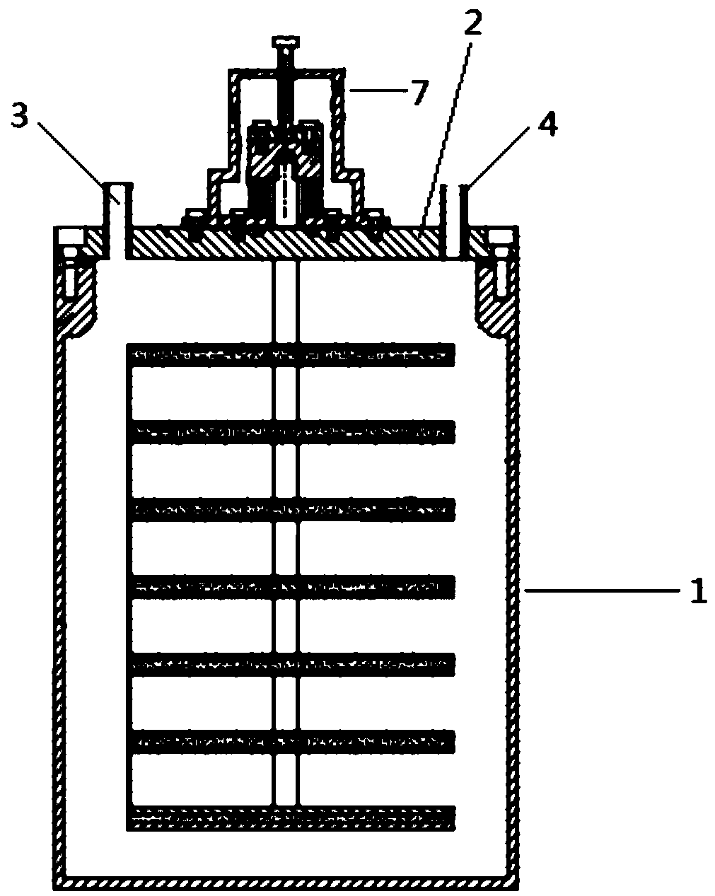
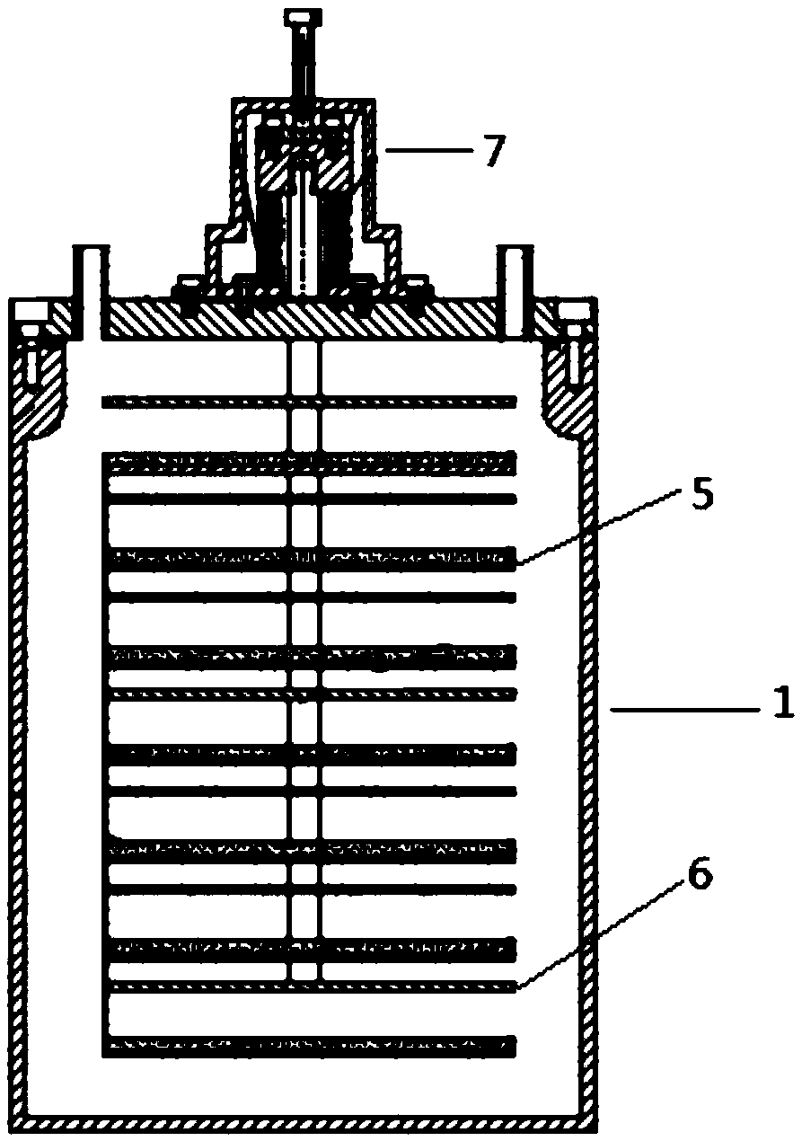
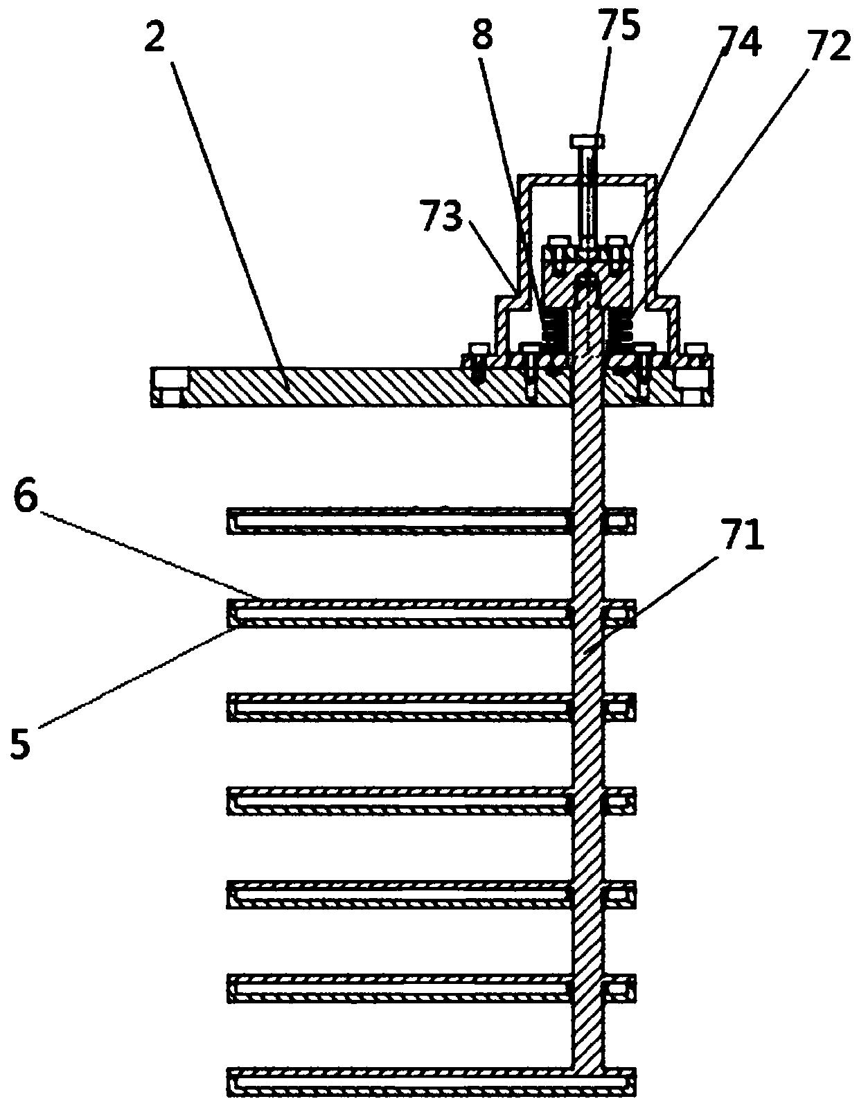
[0060] In another embodiment of the present invention, a guide hole is vertically provided in the bottle cap 2, and the air intake pipe 3 extends to the outside of the confined space through the guide hole; and the guide hole can limit the rotational freedom of the air intake pipe 3.

[0061] In the embodiment of the present invention, the degree of freedom of the intake pipe is limited by the guide hole to ensure the multi-directional rotation of the intake pipe in the confined space. Further, the tray fixed with the intake pipe can be rotated in multiple directions in the confined space, thereby facilitating Loading of solid state sources.

Embodiment 4

[0063] For the above-mentioned source bottle, the embodiment of the present invention also provides a semiconductor device, including a reaction chamber, a carrier gas pipeline, a source bottle and an air inlet pipeline, wherein the carrier gas pipeline is used to transport the carrier gas to the source bottle; For containing the solid-state source, the source bottle is the source bottle in the above embodiment; the gas inlet line is used to deliver the carrier gas and reaction gas in the source bottle to the reaction chamber.


PUM


Abstract

The invention provides a source bottle and semiconductor equipment. The source bottle comprises a bottle body and a bottle cap fixedly installed on the bottle body, the bottle body and the bottle capcan form a closed space, the bottle cap is also provided with an air inlet pipe and an air outlet pipe which are in communication with the closed space, the air inlet pipe is used for introducing carrier gas into the closed space, and the air outlet pipe is in communication with the closed space, the air outlet pipe is used for outputting a reaction precursor and the carrier gas to the outside ofthe closed space, and the source bottle further comprises a tray, a cover plate and a lifting device, the tray is arranged in the closed space and used for loading a solid source; the cover plate is arranged opposite to the tray; the lifting device is used for driving the cover plate to descend to a first position for covering the solid source on the tray; or to a second position separated from the tray. According to the source bottle, the problems of insufficient steam concentration of the solid source and scattering of the solid source in the transportation and installation process are solved.

Description

technical field [0001] The invention relates to the field of semiconductor manufacturing, in particular to a source bottle and semiconductor equipment. Background technique [0002] At present, thin film deposition reaction systems and methods are widely used in devices in various fields, such as: semiconductors, integrated circuits, solar panels, flat-panel displays, microelectronics, light-emitting diodes, and the like. Forming a thin film with a thickness of 10 μm or less than 10 μm on the surface of a substrate by chemical vapor deposition (Chemical Vapor Deposition, hereinafter referred to as CVD) technology is a common method for thin film deposition. However, in the film deposition method using atomic layer deposition (Atomic Layer Deposition, hereinafter referred to as ALD) technology, a variety of reaction gases or vapors are required to enter the reaction chamber successively and continuously in an alternative manner, and before entering the chamber, they cannot i...

Claims


Application Information

Patent Timeline
Patent Type & Authority Applications(China)
IPC IPC(8): C23C16/448
CPCC23C16/4481
Inventor 王勇飞兰云峰王帅伟
Owner BEIJING NAURA MICROELECTRONICS EQUIP CO LTD
Why Eureka
Try Eureka