
A Super-resolution Lithography Device Based on Alignment Detection and Control of Dark Field Moiré Fringes

A moiré fringe and super-resolution technology, which is applied in the photolithography process exposure device, pattern surface photolithography process, micro-lithography exposure equipment, etc., can solve the problem of unsmooth application of SP lithography and limit the application of SP lithography Scenarios and other problems, to achieve the effect of precise overlay stepping photolithography alignment and eliminating deformation-like alignment deviations

Active Publication Date: 2021-06-18
INST OF OPTICS & ELECTRONICS - CHINESE ACAD OF SCI
View PDF7 Cites 0 Cited by
  • Summary
  • Abstract
  • Description
  • Claims
  • Application Information

AI Technical Summary

Problems solved by technology

Due to the short working distance of SP lithography, the alignment method of projection lithography cannot be successfully applied to SP lithography
In addition, due to the small tool distance between the mask and the substrate, there is a force in the micro-contact state between the mask and the substrate. Under such a small gap, the distance between the mask pattern and the existing pattern on the substrate can be accurately detected and controlled. Alignment deviation, ensuring the stability and reliability of lithography effect has become a new technical problem, which limits the application scenarios of SP lithography

Method used


Image

  • A Super-resolution Lithography Device Based on Alignment Detection and Control of Dark Field Moiré Fringes
  • A Super-resolution Lithography Device Based on Alignment Detection and Control of Dark Field Moiré Fringes
  • A Super-resolution Lithography Device Based on Alignment Detection and Control of Dark Field Moiré Fringes

Examples


Embodiment Construction

[0033] In order to make the purpose, technical solution and advantages of the device of the present invention clearer, the present invention will be further described in detail below in conjunction with the accompanying drawings.

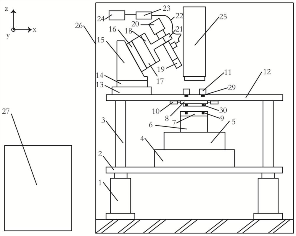
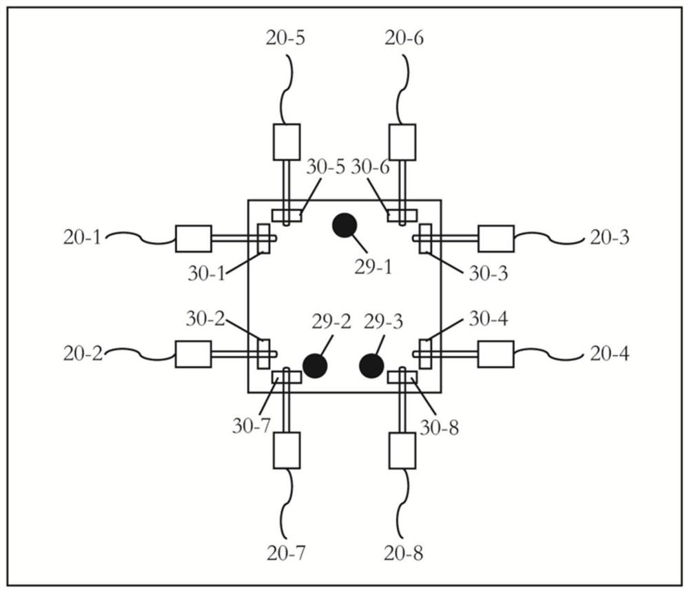
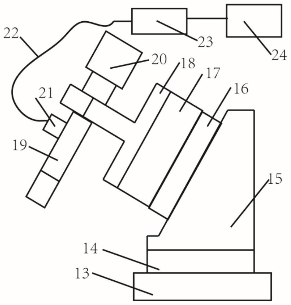
[0034] refer to figure 1 , the device is mainly composed of an active vibration isolation platform 1, a marble table 2, a support frame 3, a rough-stroke motion table 4, a six-degree-of-freedom nano-motion table 5, a substrate table 6, a substrate 7, a super-resolution photolithography mask 8, Substrate alignment mark area 9, mask deformation correction module 10, white light gap detection module 11, main substrate 12, alignment deviation detection module (including X / Y axis displacement stage 13, Tz axis rotation stage 14, tilt adapter plate 15. Z-axis translation stage 16, Rx / Ry rotary stage 17, lens holder 18, telecentric lens 19, CCD camera 20, optical fiber collimation unit 21, flexible optical fiber 22, shutter 23, alignment light source 24), ...


PUM


Abstract

The invention discloses a super-resolution lithography device based on dark field moiré fringe alignment detection and control, which includes a precise environmental control system, an active vibration isolation platform, a support frame, a light source, an alignment detection system, and a mask Deformation correction system, lithography lens module, film holder and control system. The device realizes nanoscale online alignment detection through dark-field moiré fringe diffraction imaging technology, and eliminates the alignment deviation between the mask and the substrate by controlling the nano-movement stage and the mask deformation correction system, and realizes multi-layer graphics. Engraving exposure; through the feedback control of the white light gap measurement module, precision translation stage, nanometer translation stage, and mask deformation module, the super-resolution multi-layer graphic overlay exposure lithography function is realized.

Description

technical field [0001] The invention relates to a super-resolution photolithography device based on dark-field moiré fringe alignment detection and control, and belongs to the technical field of improvement and innovation of super-resolution photolithography devices. Background technique [0002] With the rapid development of the semiconductor IC industry, IC integrated circuits continue to develop in the direction of miniaturization and higher storage density, and there is an urgent need to improve the photolithography process. The resolution and exposure efficiency of the photolithography process determine the resolution and production efficiency of the production of integrated circuit chips. The photolithography process is to transfer the pattern on the mask plate to the photoresist on the surface of the substrate through exposure operation, and then transfer the pattern to the substrate through developing, etching and other processes. Due to the effects of diffraction a...

Claims


Application Information

Patent Timeline
Patent Type & Authority Patents(China)
IPC IPC(8): G03F9/00G03F7/20
CPCG03F7/7085G03F9/7088
Inventor 罗先刚刘明刚蒲明博马晓亮高平李雄
Owner INST OF OPTICS & ELECTRONICS - CHINESE ACAD OF SCI
Learn More