Touch display panel, manufacturing method thereof and touch display device

A touch display panel, touch electrode technology, applied in the direction of instruments, electrical digital data processing, data processing input/output process, etc., can solve the problems of easy fracture of inorganic layer, metal etching residue, product short circuit, etc., to achieve Effects of reducing breakage, avoiding reaction, and avoiding short circuit

Pending Publication Date: 2020-06-30
YUNGU GUAN TECH CO LTD
View PDF0 Cites 13 Cited by
  • Summary
  • Abstract
  • Description
  • Claims
  • Application Information

AI Technical Summary

Problems solved by technology

However, when the lower film layer of the touch electrode is an inorganic layer, there is a problem that the inorganic layer in the touch function layer is relatively easy to break when bending; when

Method used


Image

  • Touch display panel, manufacturing method thereof and touch display device
  • Touch display panel, manufacturing method thereof and touch display device
  • Touch display panel, manufacturing method thereof and touch display device

Examples


Example Embodiment

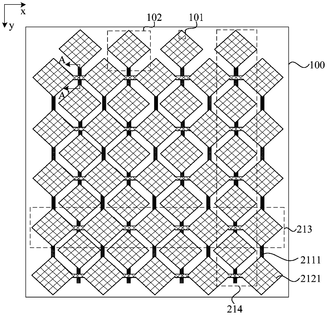
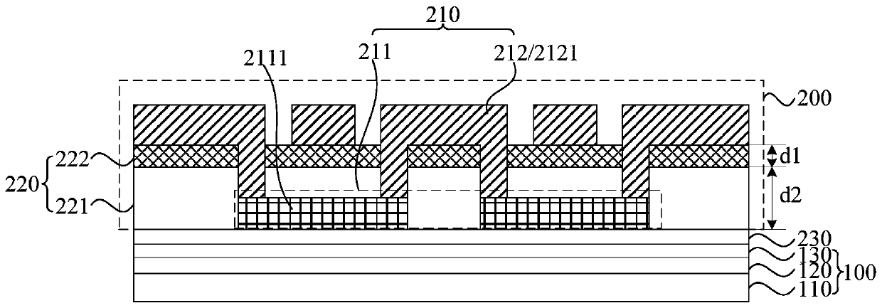
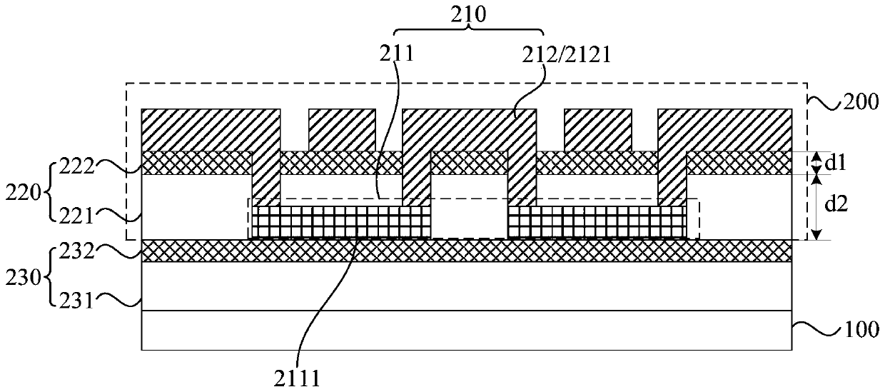
[0040] The present invention will be further described in detail below with reference to the drawings and embodiments. It can be understood that the specific embodiments described here are only used to explain the present invention, but not to limit the present invention. In addition, it should be noted that, for ease of description, the drawings only show a part but not all of the structure related to the present invention.

[0041] As described in the background art, when the underlying film layer of the touch electrode of the prior art display panel adopts an inorganic layer, there is a problem that the inorganic layer in the touch function layer is relatively easy to break when bent, and the underlying film layer of the touch electrode adopts In the case of the organic layer, there is a problem of metal etching residue during the etching of the touch function layer, resulting in a short circuit of the product. According to the inventor’s research, the reason for the above pr...


PUM

PropertyMeasurementUnit
Thicknessaaaaaaaaaa
Thicknessaaaaaaaaaa

Abstract

The embodiment of the invention discloses a touch display panel, a manufacturing method thereof and a display device. The touch display panel comprises a touch function layer, wherein the touch function layer comprises a touch electrode layer, and the touch electrode layer comprises at least one metal layer used for forming touch electrodes; the touch function layer further comprises insulating layers in one-to-one correspondence with the metal layers, wherein the insulating layers are adjacent film layers on the sides, close to the display function layer, of the corresponding metal layers, atleast one insulating layer is an insulating layer of a laminated structure, and the insulating layer of the laminated structure comprises an organic insulating layer and an inorganic insulating layerwhich are arranged in a laminated mode in the direction from the display function layer to the corresponding metal layer; the thickness of the inorganic insulating layers can be correspondingly reduced, so the flexibility of the touch display panel can be improved; moreover, etching residues caused by metal oxide generated by water vapor reaction in the metal layer and the organic insulating layer can be avoided, and etching residues caused by metal ions entering the organic insulating layer when the metal layer is formed can also be avoided, so that short circuit is avoided.

Description

technical field [0001] The embodiments of the present invention relate to the technical field of touch display, and in particular, to a touch display panel, a manufacturing method thereof, and a touch display device. Background technique [0002] With the development of display technology, the requirements for the flexibility of the display panel are getting higher and higher. [0003] In the prior art, the display panel usually includes a touch function layer, wherein the touch function layer with a metal grid touch electrode structure is widely used due to its ultra-thin and low price advantages. In the prior art, the lower layer of the touch electrode is usually an inorganic layer or an organic layer. However, when the lower film layer of the touch electrode is an inorganic layer, there is a problem that the inorganic layer in the touch function layer is relatively easy to break when bending; when the lower film layer of the touch electrode is an organic layer, there is ...

Claims


Application Information

Patent Timeline
IPC IPC(8): G06F3/041G06F3/044
CPCG06F3/0412G06F3/044G06F2203/04103G06F2203/04102G06F2203/04111
Inventor 张田超
Owner YUNGU GUAN TECH CO LTD
Why Eureka
Try Eureka