PCB capable of detecting depth of back drilling hole and detection method

A PCB board and detection method technology, which is applied in the field of PCB boards for detecting the depth of back-drilled holes, can solve the problems affecting the signal transmission and quality of PCB boards, the depth and accuracy of back-drilled holes are not easy to grasp, and increase the production cost of PCB boards, etc. To achieve the effect of reducing the scrapping of slices, optimizing the control method, and shortening the detection time

Pending Publication Date: 2020-06-30
VICTORY GIANT TECH HUIZHOU CO LTD
View PDF4 Cites 8 Cited by
  • Summary
  • Abstract
  • Description
  • Claims
  • Application Information

AI Technical Summary

Problems solved by technology

In order to prevent signal distortion and delay, it is necessary to drill out the metal in the hole without any transmission function at the end of the through hole of the PCB board to maintain signal integrity and not be disturbed. Conventional back drilling technology is used to remove some useless holes to meet h

Method used


Image

  • PCB capable of detecting depth of back drilling hole and detection method

Examples


Embodiment Construction

[0018] The present invention will be further described below in conjunction with the accompanying drawings.

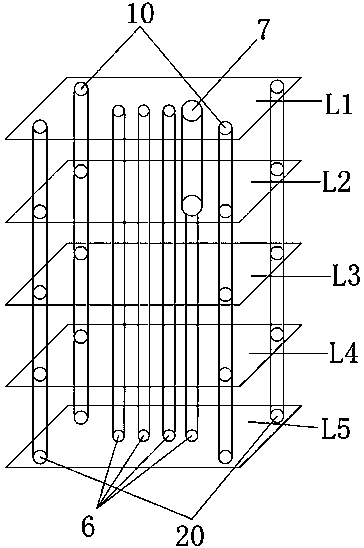
[0019] Referring to the accompanying drawings, a PCB board capable of detecting the depth of a back-drilled hole includes a PCB board formed by stacking layers of L1, L2, L3, L4 and L5 from top to bottom in sequence, and a test hole is provided on the PCB. It is a through hole, and the test holes include 2 short-circuit test holes 10 and 2 open-circuit test holes 20, and a circuit is arranged on each layer of the board, and the 2 short-circuit test holes 10 and 2 open-circuit test holes 20 form a loop connected with the circuit respectively , the PCB board is provided with at least one through-hole A6 except the test hole, copper plating in the through-hole A connects the 5-layer board for communication, and at least one through-hole A6 is provided with a back-drilled hole 7, the through-hole A is connected to The circuit of the short test hole and the circuit connecte...


PUM

PropertyMeasurementUnit
Apertureaaaaaaaaaa

Abstract

The invention discloses a PCB capable of detecting the depth of a back drilling hole. The PCB is formed by overlapping L1, L2,..., LN layers of boards (N > 2) in sequence; the PCB is provided with test holes. The test holes are through holes; the test holes comprise two short-circuit test holes and two open-circuit test holes; each layer of plate is provided with a circuit; the two short-circuit test holes and the two open-circuit test holes respectively form a communication loop with the circuit; the PCB is provided with at least one through hole A except the test holes, copper is plated in the through hole A, a back drilling hole is formed in the at least one through hole A, and the through hole A is electrically connected with a circuit connected with the short-circuit test holes and acircuit connected with the open-circuit test holes respectively. The invention further provides a detection method capable of detecting the depth of the back drill hole, the size precision of the backdrill hole is improved, the quality of the PCB is ensured, and the quality of the back drill hole is well monitored through a power-on test method.

Description

technical field [0001] The invention relates to the field of PCB boards, in particular to a PCB board capable of detecting the depth of a back-drilled hole and a detection method. Background technique [0002] With the development of the electronics industry, especially the application of HDI high-density and high-speed connection products is becoming more and more widely, the requirements for signal integrity transmission are getting higher and higher, and the back-drilling technology of PCB is also widely used. In order to prevent signal distortion and delay, it is necessary to drill out the metal in the hole without any transmission function at the end of the through hole of the PCB board to maintain signal integrity and not be disturbed. Conventional back drilling technology is used to remove some useless holes to meet high frequency and high speed. performance, but the depth and precision of the back-drilled holes are not easy to grasp. Less or more back-drilled holes w...

Claims


Application Information

Patent Timeline
IPC IPC(8): H05K3/00G01B7/26
CPCH05K3/0047G01B7/26H05K2203/0207
Inventor 黄慧张斌文志学赵启祥
Owner VICTORY GIANT TECH HUIZHOU CO LTD
Why Eureka
Try Eureka