Semiconductor device and manufacturing method thereof

A manufacturing method and semiconductor technology, applied in the direction of semiconductor/solid-state device manufacturing, semiconductor devices, electric solid-state devices, etc., can solve the problems of large variation in withstand voltage, voltage fluctuation, etc., and achieve reduced area, reduced size, and reduced horizontal distance between planes. Effect

Pending Publication Date: 2020-07-03
HANGZHOU SILAN MICROELECTRONICS
View PDF0 Cites 0 Cited by
  • Summary
  • Abstract
  • Description
  • Claims
  • Application Information

AI Technical Summary

Problems solved by technology

In the existing process, only when the design rule is greater than the critical value can the withstand voltage of t

Method used


Image

  • Semiconductor device and manufacturing method thereof
  • Semiconductor device and manufacturing method thereof
  • Semiconductor device and manufacturing method thereof

Examples


Example Embodiment

[0049] Hereinafter, the present disclosure will be described in more detail with reference to the accompanying drawings. In the various figures, identical elements are indicated with similar reference numerals. For the sake of clarity, various parts in the drawings have not been drawn to scale. Also, some well-known parts may not be shown.

[0050] In the following, many specific details of the present invention are described, such as device structures, materials, dimensions, processing techniques and techniques, for a clearer understanding of the present invention. However, the invention may be practiced without these specific details, as will be understood by those skilled in the art.

[0051] The invention can be embodied in various forms, some examples of which are described below.

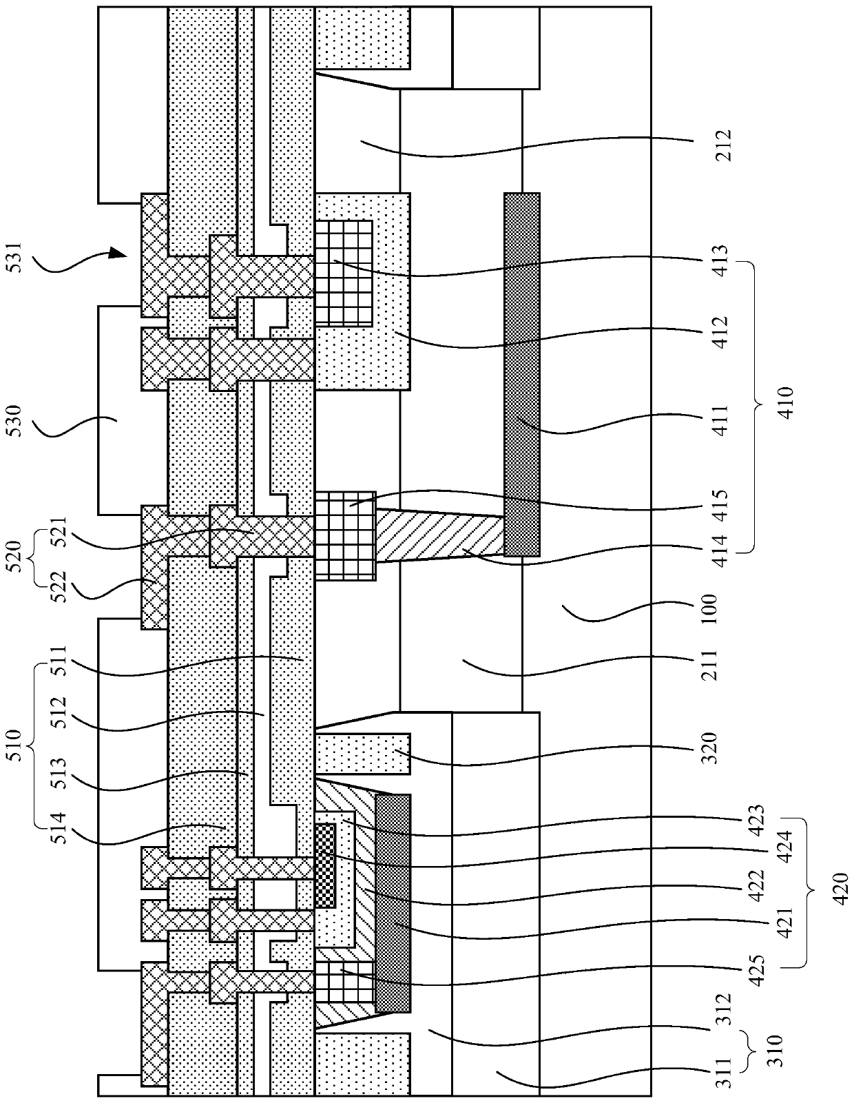
[0052] figure 1 A schematic structural diagram of a semiconductor device according to an embodiment of the present disclosure is shown.

[0053] like figure 1 As shown, the semiconductor...


PUM


Abstract

The invention discloses a semiconductor device and a manufacturing method thereof. The semiconductor device includes: a substrate; a first epitaxial layer which is positioned on the substrate; a second epitaxial layer which is positioned on the first epitaxial layer; a high-voltage device which is located in the first epitaxial layer and the second epitaxial layer; a low-voltage device which is located in the second epitaxial layer; and a first isolation region which is located in the first epitaxial layer and the second epitaxial layer, and the first isolation region is used for isolating thehigh-voltage device and the low-voltage device. The low-voltage device is manufactured in the second epitaxial layer, so that the size of the low-voltage device is greatly reduced, and the overall area of the chip is remarkably reduced.

Description

technical field [0001] The present disclosure relates to the technical field of semiconductors, and more particularly, to a semiconductor device and a manufacturing method thereof. Background technique [0002] The manufacturing cost of an integrated circuit chip is usually determined by the chip area and the number of lithography layers in the tape-out. The smaller the chip area and the fewer lithography layers, the lower the cost and the lower the selling price. Different methods can be used to reduce the cost of chip manufacturing, such as reducing the area and the number of photolithography layers at the same time, or greatly reducing the area and limitedly increasing the number of photolithography layers, or greatly reducing the number of photolithography layers and limitedly increasing the area . [0003] In the prior art, the way to reduce the chip area can only be achieved by adjusting the process and reducing the size of the rules. For low-voltage digital circuits...

Claims


Application Information

Patent Timeline
IPC IPC(8): H01L27/02H01L29/06H01L21/82
CPCH01L21/82H01L27/0203H01L29/0603H01L29/0684
Inventor 冯荣杰
Owner HANGZHOU SILAN MICROELECTRONICS
Why Eureka
Try Eureka