Semiconductor device lead assembling equipment

An assembly equipment and semiconductor technology, which is applied in semiconductor devices, semiconductor/solid-state device manufacturing, electric solid-state devices, etc., can solve problems such as missing insertion, reverse insertion, and prone to strain

Pending Publication Date: 2020-07-07
乐山希尔电子股份有限公司
View PDF0 Cites 3 Cited by
  • Summary
  • Abstract
  • Description
  • Claims
  • Application Information

AI Technical Summary

Problems solved by technology

Among them, the three-dimensional semiconductor discrete device has four outer leads perpendicular to the heat dissipation surface. It needs to be assembled and welded by multiple parts in the production process. The traditional process us

Method used


Image

  • Semiconductor device lead assembling equipment
  • Semiconductor device lead assembling equipment
  • Semiconductor device lead assembling equipment

Examples


Embodiment 1

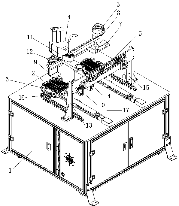
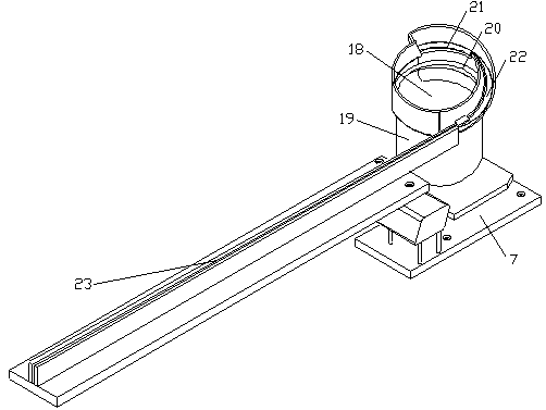
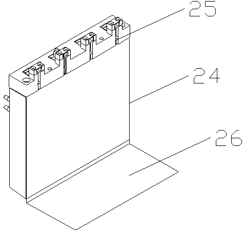
[0037] As a most basic embodiment of the present invention, this embodiment discloses a semiconductor device lead assembly equipment, such as figure 1 As shown, it includes a cabinet 1, and the cabinet 1 includes a work surface 2, and the work surface 2 is provided with a lead wire arrangement device 3, a lead wire grasping device 4, an eagle eye identification device 5 and a lead wire installation device 6, and the The lead wire arrangement device 3 includes a vibrating plate mounting base 7, a vibrating plate 8 and a jacking mechanism 9; the lead wire grabbing device 4 includes a manipulator mounting seat 10, a four-axis manipulator 11 and a lead wire grabbing mechanism 12; the eagle eye identification device 5 includes an eagle eye mounting frame 13, an eagle eye moving mechanism 14, and a CCD industrial camera 15; the lead wire installation device 6 includes a graphite box positioning plate mechanism 16 and a graphite box transmission mechanism 17; a PLC controller is arran...

Embodiment 2

[0040] As a preferred embodiment of the present invention, this embodiment discloses a semiconductor device lead assembly equipment, such as figure 1 As shown, it includes a cabinet 1, and the cabinet 1 includes a work surface 2, and the work surface 2 is provided with a lead wire arrangement device 3, a lead wire grasping device 4, an eagle eye identification device 5 and a lead wire installation device 6, and the The lead wire arrangement device 3 includes a vibrating plate mounting base 7, a vibrating plate 8 and a jacking mechanism 9; the lead wire grabbing device 4 includes a manipulator mounting seat 10, a four-axis manipulator 11 and a lead wire grabbing mechanism 12; the eagle eye identification device 5 includes an eagle eye mounting frame 13, an eagle eye moving mechanism 14, and a CCD industrial camera 15; the lead wire installation device 6 includes a graphite box positioning plate mechanism 16 and a graphite box transmission mechanism 17; a PLC controller is arrang...


PUM


Abstract

The invention discloses semiconductor device lead assembling equipment, and relates to the technical field of semiconductor device production. The equipment comprises a cabinet, wherein the cabinet comprises a working table, the working table is provided with a lead arrangement device, a lead grabbing device, an eagle eye recognition device and a lead mounting device, and the lead arrangement device comprises a vibration disc mounting base, a vibration disc and a jacking mechanism; the lead grabbing device comprises a manipulator mounting base, a four-axis manipulator and a lead grabbing mechanism; the eagle eye recognition device comprises an eagle eye mounting frame, an eagle eye moving mechanism and a CCD industrial camera; the lead mounting device comprises a graphite box positioning disc mechanism and a graphite box transmission mechanism; a PLC is arranged in the cabinet, and the lead arrangement device, the lead grabbing device, the eagle eye recognition device and the lead mounting device are electrically connected with the PLC. The equipment has the advantages of improving the labor efficiency, reducing the labor intensity, improving the product quality and the like.

Description

technical field [0001] The invention belongs to the technical field of semiconductor device production, and in particular relates to a semiconductor device lead assembly equipment. Background technique [0002] Semiconductor devices are widely used in rail transit, home appliances, new energy, power supplies, frequency converters, consumer electronics, computers and peripherals, network communications, automotive electronics, LEDs and other fields. Semiconductor discrete devices are composed of chips, soldering materials, lead frames, and packaging materials. Among them, the three-dimensional semiconductor discrete device has four outer leads perpendicular to the heat dissipation surface. It needs to be assembled and welded by multiple parts in the production process. The traditional process uses manual installation of the leads, which is inefficient and labor-intensive. , arms and other parts are prone to strain, and if employees are not careful, it is also prone to qualit...

Claims


Application Information

Patent Timeline
IPC IPC(8): H01L21/60H01L21/677H01L21/68H01L21/683
CPCH01L21/67742H01L21/681H01L21/6838H01L24/85H01L2224/852
Inventor 邓华鲜
Owner 乐山希尔电子股份有限公司
Why Eureka
Try Eureka