Semiconductor device and preparation method thereof

A semiconductor and device technology, applied in the field of semiconductor devices and their preparation, can solve the problems of small saturation current and large dynamic on-resistance

Active Publication Date: 2020-07-07
DYNAX SEMICON
View PDF3 Cites 0 Cited by
  • Summary
  • Abstract
  • Description
  • Claims
  • Application Information

AI Technical Summary

Problems solved by technology

[0004] In view of this, an embodiment of the present invention provides a semiconductor device and its preparation method to solve the technical problems in the prior art that the semiconductor device has a large dynamic on-resistance and a small saturation current due to electrons trapped by defects in the buffer layer.

Method used


Image

  • Semiconductor device and preparation method thereof
  • Semiconductor device and preparation method thereof
  • Semiconductor device and preparation method thereof

Examples


Embodiment Construction

[0053]In order to make the purpose, technical solution and advantages of the present invention clearer, the technical solution of the present invention will be fully described below through specific implementation in combination with the drawings in the embodiments of the present invention. Apparently, the described embodiments are some embodiments of the present invention, rather than all embodiments. Based on the embodiments of the present invention, all other embodiments obtained by persons of ordinary skill in the art without making creative efforts, All fall within the protection scope of the present invention.

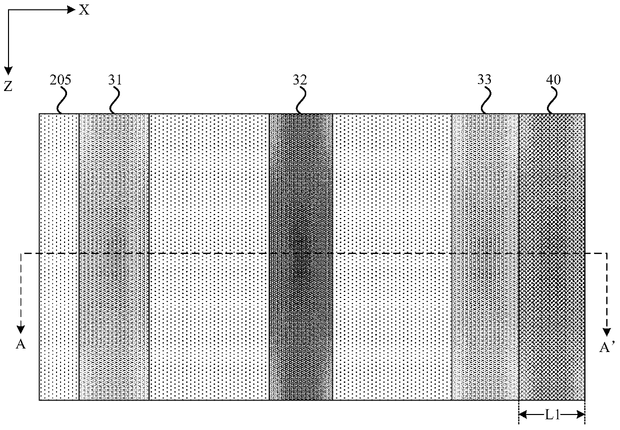
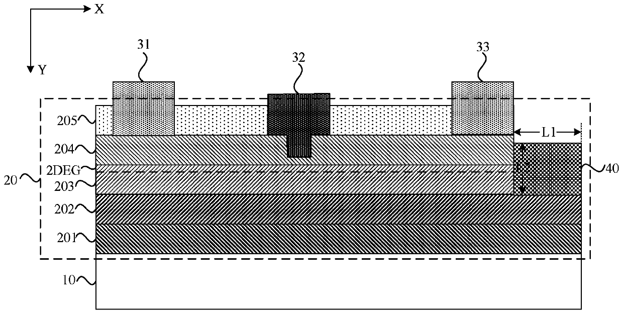
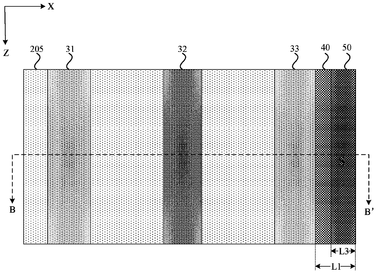
[0054] An embodiment of the present invention provides a semiconductor device, including a substrate; a multilayer semiconductor layer located on one side of the substrate, wherein the multilayer semiconductor layer includes a buffer layer, a channel layer, and a barrier layer sequentially located on one side of the substrate; The source, gate and drain on the si...


PUM

PropertyMeasurementUnit
thicknessaaaaaaaaaa
thicknessaaaaaaaaaa
heightaaaaaaaaaa

Abstract

The embodiment of the invention discloses a semiconductor device and a preparation method thereof. The semiconductor device comprises: a substrate, multiple semiconductor layers which are positioned on one side of the substrate and comprise a buffer layer, a channel layer and a barrier layer which are sequentially positioned on one side of the substrate; a source electrode, a grid electrode and adrain electrode which are located on the side, away from the substrate, of the multiple semiconductor layers, wherein the grid electrode is located between the source electrode and the drain electrode; and P-type material layer located in the multiple semiconductor layers and located on the side, away from the grid electrode, of the drain electrode, the lower surface of the P-type material layer extends to the surface of the side, close to the channel layer, of the buffer layer or extends into the buffer layer, and the P-type material layer is electrically connected with the drain electrode. AP-type material layer is arranged to be electrically connected with a drain electrode; under forward bias, the P-type material layer injects holes into the buffer layer to neutralize electrons boundby traps caused by lattice defects or doping in the buffer layer, so that the speed of separating the electrons from the buffer layer is increased, the saturation current of the semiconductor device is improved, the dynamic on-resistance of the semiconductor device is reduced, and the performance of the semiconductor device is improved.

Description

technical field [0001] Embodiments of the present invention relate to the technical field of semiconductors, and in particular to a semiconductor device and a manufacturing method thereof. Background technique [0002] In recent years, GaN-based high electron mobility transistors (HEMTs) have developed rapidly, and the wurtzite structure AlGaN / GaN HEMTs have the best development prospects. HEMTs may also be referred to as Modulation Doped Field Effect Transistors (MODFETs) or Heterojunction Field Effect Transistors (HFETs). Its on-resistance and parasitic capacitance are small, the switching speed is fast, and the thermal stability is good. It is a high-temperature, high-frequency and high-power device that is currently booming. [0003] At present, GaN-based HEMT devices have entered the practical stage and play a key role, but there are still many reliability problems, which seriously restrict the popularization and further development of devices. Among them, because the...

Claims


Application Information

Patent Timeline
Patent Type & Authority Applications(China)
IPC IPC(8): H01L29/778H01L29/06H01L21/335
CPCH01L29/7787H01L29/66462H01L29/0688
Inventor 钱洪途韩啸
Owner DYNAX SEMICON
Why Eureka
Try Eureka