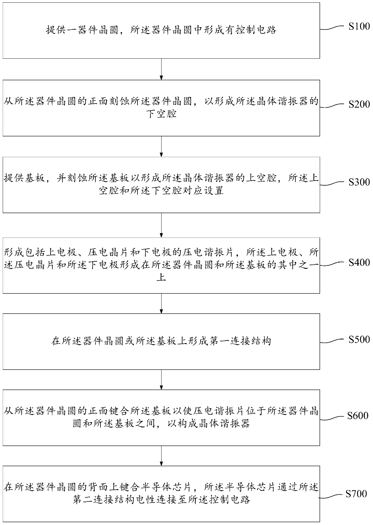
Integrated structure of crystal resonator and control circuit and integration method thereof
A crystal resonator and control circuit technology, applied in the direction of electrical components, impedance networks, etc., can solve the problems of large size and difficult integration
- Summary
- Abstract
- Description
- Claims
- Application Information
AI Technical Summary
Problems solved by technology
Method used
Image

Examples
Embodiment 2
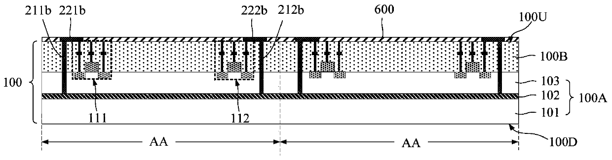
[0122] The difference from the first embodiment is that in this embodiment, the upper electrode 530 , the piezoelectric wafer 520 and the lower electrode 510 of the piezoelectric resonant sheet 500 are all formed on the front surface of the device wafer 100 , and the The piezoelectric resonator sheet 500 covers the opening of the lower cavity 120, and the formed crystal resonator is electrically connected to the control circuit in the device wafer 100, and then a bonding process is performed, so that the upper cavity 310 corresponds to the above-mentioned The side of the piezoelectric resonator plate 500 facing away from the lower cavity 120 forms a crystal resonator, thereby realizing the integrated setting of the crystal resonator and the control circuit.
[0123] In this embodiment, for providing a device wafer with a control circuit and a method for forming a lower cavity in the device wafer, reference may be made to Embodiment 1, and details are not described here.
[012...
Embodiment 1
[0141] In the first embodiment and the second embodiment, the piezoelectric resonant sheet including the upper electrode, the piezoelectric wafer and the lower electrode are all formed on the substrate or the device wafer. The difference from the above embodiment is that in this embodiment, the upper electrode and the piezoelectric wafer are formed on the substrate, and the lower electrode is formed on the device wafer.
[0142] Figure 3a ~ Figure 3d This is a schematic structural diagram of the method for integrating a crystal resonator and a control circuit in the third embodiment of the present invention in the manufacturing process. The following describes the steps of forming a crystal resonator in this embodiment in detail with reference to the accompanying drawings.
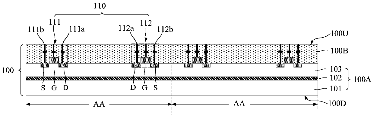
[0143] First refer to Figure 3a As shown, a device wafer 100 is provided, the device wafer 100 has a control circuit formed therein, and a lower electrode 510 is formed on the front side of the device w...
PUM
 Abstract
Description
Claims
Application Information