Photoacoustic spectrometry detection chip sensor and manufacturing method
A technology for detecting chips and photoacoustic spectroscopy, which is used in color/spectral characteristic measurement, instruments, measuring devices, etc., can solve the problems of poor integration and stability of micro-vibration sensors, and achieve easy production and solution of optical fiber distributed sensing systems. Integration problems, the effect of simple and firm structure
- Summary
- Abstract
- Description
- Claims
- Application Information
AI Technical Summary
Problems solved by technology
Method used
Image

Examples
Embodiment
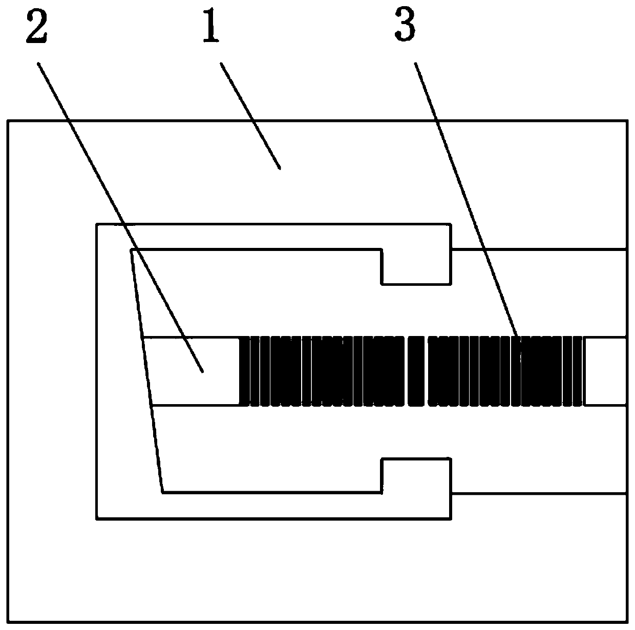
[0026] A chip sensor for photoacoustic spectrum detection, comprising: a vibration transduction structure 1, an optical waveguide 2 and a phase shift waveguide grating 3, the optical waveguide 2 is arranged on the vibration transduction structure 1, the optical waveguide 2 is a three-layer waveguide layer, including a lining Bottom, light guide layer and cladding layer, vibration transduction structure 1 as the substrate of optical waveguide 2, the light guide layer of optical waveguide 2 is rare earth doped silica, the cladding layer of optical waveguide 2 is silicon dioxide, phase shift The waveguide grating 3 is written in the light guiding layer of the optical waveguide 2 .
[0027] Wherein, the optical waveguide 2 is formed on the vibration transducing structure 1 through a moCVD process. The phase-shifted waveguide grating 3 is written in the optical waveguide 2 using UV lithography technology, and the phase shift of the phase-shifted waveguide grating 3 is π. The vibra...
PUM
 Abstract
Description
Claims
Application Information