
Display substrate and manufacturing method thereof, display panel and display device

A technology for display substrates and display panels, which is used in semiconductor/solid-state device manufacturing, diodes, semiconductor devices, etc., and can solve the problems of thick QD-OLED, thick retaining walls, and inability to make the protective layer thin, so as to ensure the display effect. , the effect of reducing the thickness

Active Publication Date: 2020-07-10
BOE TECH GRP CO LTD
View PDF8 Cites 1 Cited by
  • Summary
  • Abstract
  • Description
  • Claims
  • Application Information

AI Technical Summary

Problems solved by technology

Due to the limitations of the manufacturing process, the protective layer cannot be made thin, so that the thickness of the final barrier is thicker, resulting in a thicker thickness of the entire QD-OLED

Method used


Image

  • Display substrate and manufacturing method thereof, display panel and display device
  • Display substrate and manufacturing method thereof, display panel and display device
  • Display substrate and manufacturing method thereof, display panel and display device

Examples


Embodiment Construction

[0041] In order to make the objectives, technical solutions and advantages of the present disclosure clearer, the following further describes the embodiments of the present disclosure in detail with reference to the accompanying drawings.

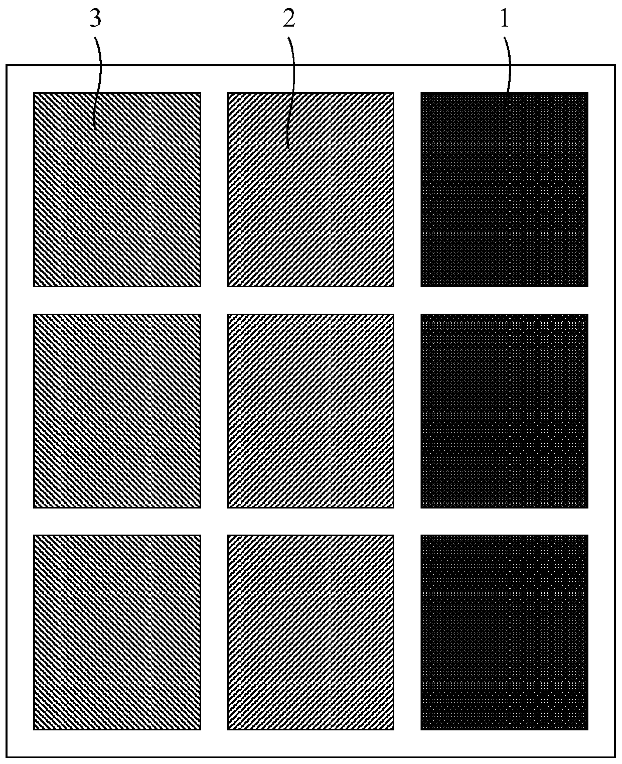
[0042] figure 1 It is a partial structural diagram of a display panel provided by an embodiment of the present disclosure. See figure 1 , The display substrate 10 has a plurality of pixel regions. The plurality of pixel regions include a green pixel region 1, a red pixel region 2 and a blue pixel region 3.

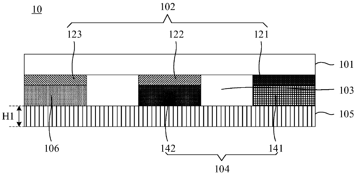
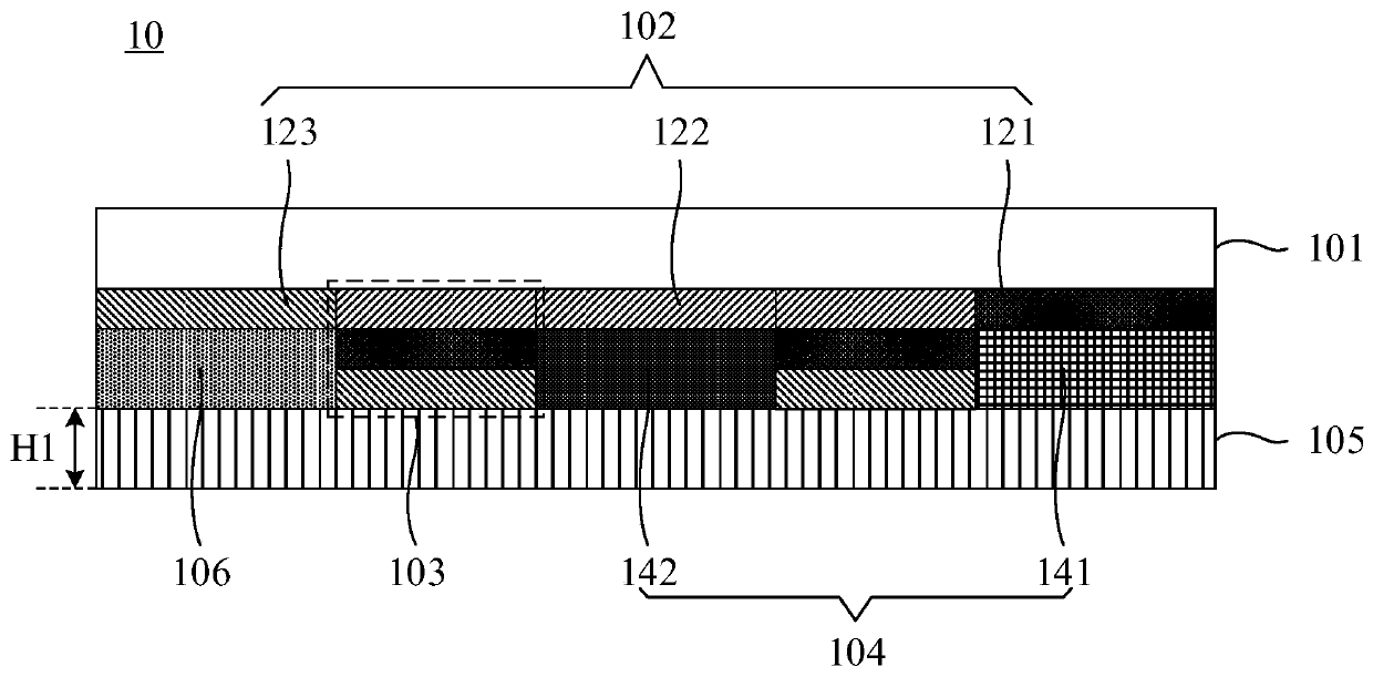
[0043] figure 2 It is a schematic cross-sectional view of a display substrate provided by an embodiment of the present disclosure. See figure 2 , The display substrate 10 includes a cover 101, a plurality of color filter layers 102 located on the cover 101 and corresponding to a plurality of pixel regions, a barrier 103 located on the cover 101 and between adjacent pixel regions, And a plurality of quantum dot films 104 on the color filt...


PUM

PropertyMeasurementUnit
thicknessaaaaaaaaaa
thicknessaaaaaaaaaa
thicknessaaaaaaaaaa

Abstract

The invention relates to a display substrate and a manufacturing method thereof, a display panel and a display device, and belongs to the field of displays. The display substrate is provided with a plurality of pixel areas. The display substrate comprises a cover plate, a color filter layer, retaining walls and a plurality of quantum dot films, wherein the color filter layer is located on the cover plate and corresponds to the pixel areas, the retaining walls are located on the cover plate and located between the adjacent pixel areas, the quantum dot films are located on the color filter layer, and the quantum dot films correspond to at least part of the pixel areas. The retaining wall is made of at least one of a photochromic material or a filtering material. When encountering light emitted from the interior of the display device, the photochromic material is converted into colors capable of blocking the light, and the light filtering material can filter the light of each color, so that shading is realized. When the material is used for manufacturing the retaining wall, the retaining wall can be manufactured to be thinner, so that the thickness of the retaining wall is smaller than that of the retaining wall formed by the black matrix and the protective layer, and the thickness of the display device can be reduced.

Description

Technical field [0001] The present disclosure relates to the field of displays, in particular to a display substrate and a manufacturing method thereof, a display panel and a display device. Background technique [0002] Quantum Dot Organic Light-Emitting Display (English: Quantum Dot Organic Light-Emitting Display, referred to as: QD-OLED) uses blue light as a light source, and red quantum dots (English: Quantum Dot Red) are arranged in the red pixel unit and the green pixel unit of the display panel respectively. , Abbreviation: QD-R) film and green quantum dot (English: Quantum DotGreen, abbreviation: QD-G) film, red quantum dot film and green quantum dot film can respectively convert blue light into red light and green light. [0003] Exemplarily, the QD-OLED display panel may include a QD-OLED array substrate, a quantum dot film located on the QD-OLED array substrate, a color filter layer and a barrier wall, and the color filter layer and barrier wall. The cover plate, the co...

Claims


Application Information

Patent Timeline
Patent Type & Authority Applications(China)
IPC IPC(8): H01L27/32H01L51/52H01L51/56
CPCH10K59/38H10K50/86H10K71/00Y02E10/549
Inventor 张星韩影
Owner BOE TECH GRP CO LTD
Learn More