Surface treatment method for stripping single crystal thin film through ion implantation

A single crystal thin film and ion implantation technology, which is applied in cleaning methods and appliances, chemical instruments and methods, piezoelectric/electrostrictive/magnetostrictive devices, etc., can solve problems such as changes in wettability of thin films, and achieve single crystal quality The effect of improving and simplifying complexity and reducing secondary damage

Active Publication Date: 2020-07-10
UNIV OF ELECTRONICS SCI & TECH OF CHINA
View PDF11 Cites 3 Cited by
  • Summary
  • Abstract
  • Description
  • Claims
  • Application Information

AI Technical Summary

Problems solved by technology

[0005] In view of the above existing problems or deficiencies, in order to solve the problem of subsequent application due to poor repair or removal methods for the damaged layer of the single crystal film stripped by ion implantation, the present invention provides a surface treatment method for ion implantation stripped single crystal film, For the single crystal thin film stripped by ion implantation, first use argon ion etching to accurately remove the surface damage layer, and then use oxygen plasma cleaning technology to treat the surface of the film, which solves the infiltration of the film due to oxygen vacancy defects after argon ion etching The problem of property change has greatly improved the subsequent application of single crystal thin film

Method used


Image

  • Surface treatment method for stripping single crystal thin film through ion implantation
  • Surface treatment method for stripping single crystal thin film through ion implantation
  • Surface treatment method for stripping single crystal thin film through ion implantation

Examples


Embodiment 1

[0024] The surface treatment method of the ion implantation peeling single crystal thin film of the present embodiment comprises the following steps:

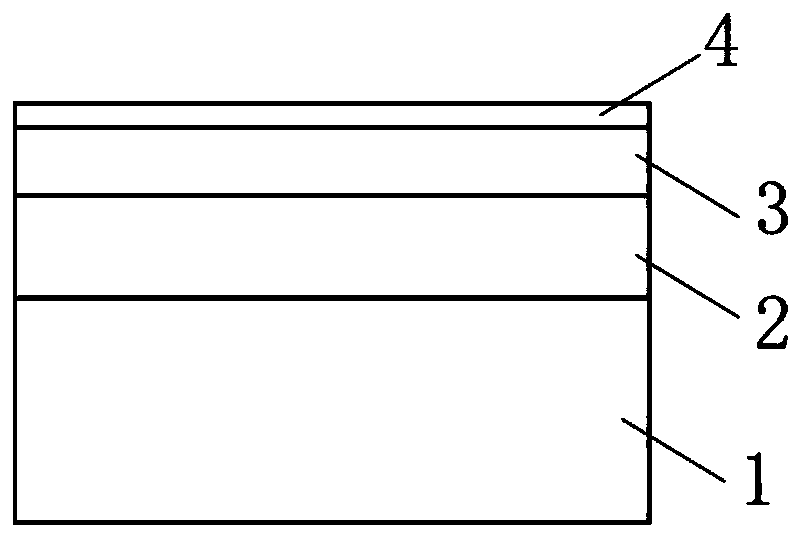
[0025] Such as figure 1 As shown, the single crystal piezoelectric thin film prepared by ion implantation stripping technology is processed, and the single crystal thin film includes a surface damage layer 4, a single crystal thin film layer 3, a bonding layer 2, and a substrate 1 from top to bottom;

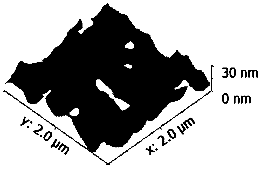
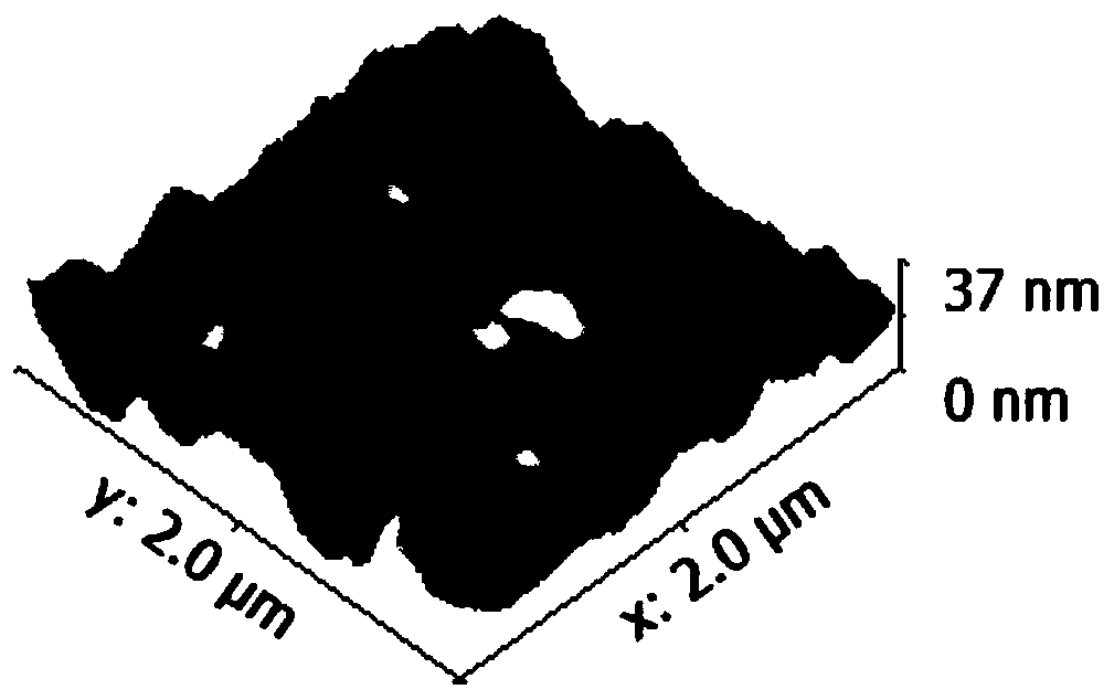
[0026] Step 1. For the monocrystalline piezoelectric thin film prepared by ion implantation stripping technology, the surface damaged layer is accurately removed by argon ion etching method.

[0027] The single crystal film prepared by ion implantation stripping technology is placed in the working chamber of the ion source, the thickness of the surface damage layer is 100nm-130nm, the beam voltage is set to 200V-500V, the beam current is 4mA-30mA, and the accelerating voltage is 40V-100V; the thickness range of the surface damag...


PUM

PropertyMeasurementUnit
thicknessaaaaaaaaaa
thicknessaaaaaaaaaa
thicknessaaaaaaaaaa

Abstract

The invention belongs to the technical field of single crystal thin films, and particularly relates to a surface treatment method for stripping a single crystal thin film through ion implantation. According to the surface treatment method for stripping the single crystal thin film through ion implantation, argon ion etching is selected for accurately removing a damaged layer on the surface of thesingle crystal thin film prepared through the ion implantation stripping technology; and besides, the problems of oxygen vacancy defects and surface modification of the film after the damaged layer isremoved are solved by respectively controlling the oxygen flux, the working power and the working parameters of the cleaning time in the oxygen plasma cleaning process, the cleaning effect is verified through the contact angle test, and finally, the single crystal thin film is completely infiltrated, so that the subsequent preparation of a graphical device structure is facilitated. According to the method, the single crystal quality of the single crystal thin film is greatly improved, the introduced secondary damage is minimum, and the process complexity is simplified.

Description

technical field [0001] The invention belongs to the technical field of single crystal thin films, and in particular relates to a surface treatment method for peeling off single crystal thin films by ion implantation. Background technique [0002] With the development of device integration, due to the limitation of volume and size, single crystal bulk materials gradually develop into single crystal thin films. Although ion implantation stripping technology can prepare single crystal thin films with various orientations, high-energy ions occur at the end of the range. Due to the scattering effect, there is a surface damage layer with a certain roughness on the surface of the film, which leads to the degradation of the single crystal quality and device performance of the single crystal film. In addition, the surface state of single crystal thin films is crucial to the preparation of patterned devices, and even affects the performance of devices. [0003] At present, various me...

Claims


Application Information

Patent Timeline
Patent Type & Authority Applications(China)
IPC IPC(8): H01L41/253H01L41/332H01L21/02H01L21/66H01L21/67B08B7/00
CPCH01L21/67253H01L22/12H01L21/02057B08B7/00H10N30/04H10N30/082
Inventor 罗文博方远苹帅垚吴传贵张万里
Owner UNIV OF ELECTRONICS SCI & TECH OF CHINA
Why Eureka
Try Eureka